8 PCB Grounding Rules to Live Your Engineering Life By
Grounding isn’t all that important, right? It’s just the foundation that we build all of our electronic designs on. But what about those signals! The truth is, grounding is the most important part of your entire design, and we all tend to ignore it until it becomes a huge problem. Without a stable ground, you’ll never pass clean signals from one device to another.
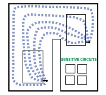
Maybe you’ve designed a digital device with some variance in your ground and data can still move safely around. However, consider something like a high-reliability medical system. If that device gets zapped with a high-voltage ESD charge, you better hope you properly designed your ground. In sensitive electronic designs such as these, proper grounding can mean the difference between life and death.
Here are 8 PCB grounding rules to live your engineering life by, keep them in your back pocket!
#1 – Leave nothing unattached
Nothing should remain unattached on your PCB layout. If there’s an open space on your board, fill it with copper and vias to connect with your ground plane. This will create a structured path for all of your signals to efficiently get to ground.
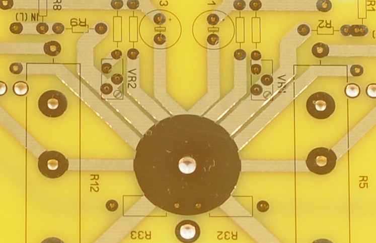
#2 – Never slice up your ground layer
Most engineers working on four layer boards will have a dedicated ground layer. This works great as long as you don’t route traces on this layer. Once you do, you’ve effectively created a ground current loop. Keep your ground layer whole at all times.
#3 – Always provide a common ground point
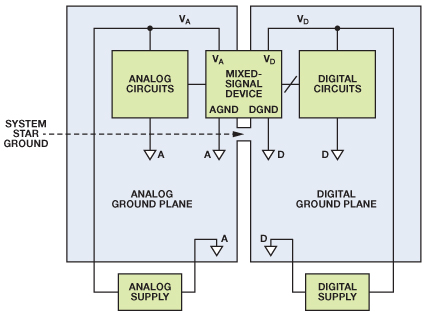
An electronics system, whether that’s a single or a multi-board system, needs a single point for all grounds to come together. This might be the metal frame on a chassis or a dedicated ground layer on your PCB. You’ll commonly hear this referred to this common ground point as star grounding.
#4 – Minimize series vias
Be sure to minimize series vias on your ground paths and instead send component grounds directly to your dedicated ground plane. The more vias you add to your board the more impedance you have to deal with. This is especially important for fast transient currents that can turn an impedance path into a voltage differential.
#5 – Grounding before routing
A poorly designed ground puts your entire device at risk. The same can’t be said for messing up a single signal. Be sure to properly design your ground first before doing any routing. This will serve as the foundation for your entire routing process.
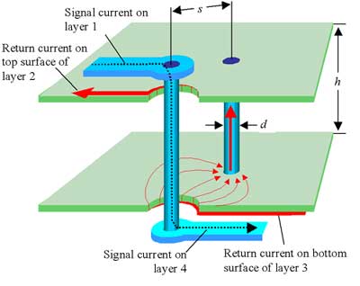
#6 – Know where your currents are going
Many designers only think about where their signal is traveling to, but every signal has a return path to take through ground. Both the sending and return path of your signal will have the same current which can affect power stability and ground bounce. You can use Kirchhoff’s Current Law to understand how current will travel through your circuit.
#7 – Plan for dynamic variance between grounds
Always plan for dynamic variance when sending ground connections between boards in a multi-board system. This is especially true when working on applications that require long-distance cables. For these situations, you can use low voltage differential signals, optical isolators, and common-mode chokes to keep variance under control.
#8 – Mind your mixed-signal floor planning
The analog parts of your board need to be kept separate. This includes analog-to-digital converters and digital-to-analog converters. When designing the “floor plan” of your PCB, be sure to keep these areas isolated. An ADC’s ground can be tied back to a common ground point where digital signals can be passed to other parts of your PCB.
When In Doubt, Ground It Out
Ground is the foundation of your entire electronics house. It’s easy to forget about this with all the focus on signal routing. However, without a clear return path, all that time spent worrying about signals will have gone to waste. Don’t ignore your ground until it becomes a problem, make it your priority! Live by the 8 rules above, and you’ll have a strong foundation to grow on for the rest of your engineering life.
Subscribe today and