& Construction

Integrated BIM tools, including Revit, AutoCAD, and Civil 3D
& Manufacturing

Professional CAD/CAM tools built on Inventor and AutoCAD
9 min read
Do you ever get tired of designing the same old square or rectangular-shaped circuit board? Today’s PCBs sometimes feel like a creation straight out of the Industrial Revolution, those perfectly square boxes that fit nice and evenly down an assembly line. This mentality doesn’t just extend into how, we as electrical engineers, design today. It also penetrates our mentalities and how we’re taught to think about electronics as flat, two-dimensional realities.
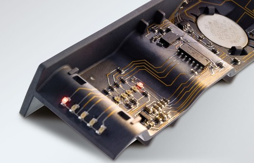
All of this is starting to change. We’re not talking about another PCB here. We’re talking about circuitry and a mechanical enclosure coming together as one complete product experience. Is this the Future of Making Things, and if so, how is it going to affect your life? Molded interconnect devices (MIDs) are here, and they’re set to change the future of engineering as we know it.
MIDs aren’t actually new. They were introduced into the world almost 20 years ago and were met with a ton of enthusiasm. Resin makers rushed out to gather the needed materials, and manufacturers attempted to adopt an entirely new set of tooling techniques to meet these new design challenges. But for whatever reason, MIDs never caught on. Maybe the change was just too much at the time, or the costs were prohibitive. And so MIDs slowly slunk into the backdrop of engineering, waiting for the right time to resurface.
Now in 2017, the demand for MIDs are growing faster than ever. But what makes this time different than 20 years ago? Miniaturization. We’re not walking around with large, brick-shaped cell phones anymore. These days, we have devices that can fit into our pockets or strap onto our wrists with a dizzying amount of capabilities.

To make sophisticated devices this small, using your conventional square-shaped circuit board that fits within your traditional mechanical enclosure just doesn’t do it. The two worlds of mechanical and electrical need to come together to meet the needs of our miniaturized and complex world.
This is the problem that MIDs are trying to solve. These devices do away with the traditional FR4 fiberglass that you’ll find in a typical PCB and instead replace it with thermoplastics. With MIDs, you can bring mechanical and electrical engineering together into a complete product, combining the circuitry, housing, connectors, and cables into one whole part. In the world of MIDs, there isn’t a separate circuit board or an enclosure anymore; they’re all just the same.
For the electronics designer, you’ll no longer be designing circuitry in a flat, square surface. Instead, you’ll use the curvature and rounded corners of a three-dimensional space as the playground for all of your components and traces. Sound a little crazy? MIDs are already being made all around the world.
There are already a ton of devices that you might not even know about that are MIDs. Take for example something simple like the security shield for ATMs. Behind that big chunk of plastic is actually a dizzying amount of traces embedded inside the enclosure, helping to protect against intrusion without requiring a physical circuit board. Beyond ATM security, MIDs are in use in all types of industries, including:
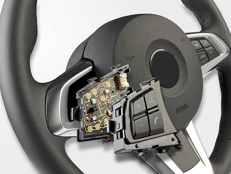
Today’s vehicles depend on a ton of sensors and electronic components to offer new functionality and safety for passengers. Take for example a steering wheel. In the past, you needed a wire harness to connect the physical molding of the wheel to its circuit board and surrounding buttons. But with MIDs? Now you can design a wheel with electronic circuitry embedded on the molding without the need for any wire harness.

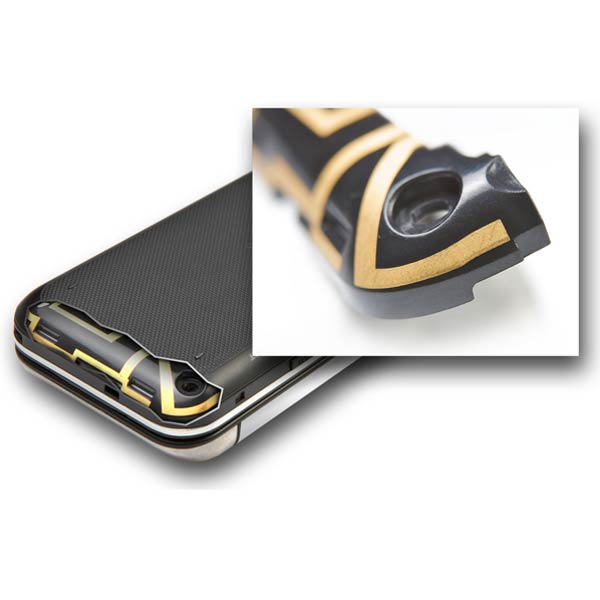
Our consumer devices just seem to keep getting thinner every year while packing in more and more functionality. But how can you keep up with more functions into a smaller package? With MIDs. Take for example something like a smartphone that requires an antenna. Rather than needing to design a stand-alone antenna, you can integrate one within the mechanical enclosure with MIDs. This ends up saving much-needed space.

Healthcare relies on many sensors and data to make sense of our health. And these days, mobile diagnostic products allow people to monitor their glucose levels or to dispense medications. But how do you make portable and potentially life-saving medical devices in increasingly smaller packages? With MIDs. Siemens already produces a pair of hearing aids using MIDs that embeds all of the circuitry and audio equipment directly within the enclosure without needing a physical circuit board.

Last but not least, you can’t forget about the future of connected devices that we’re all chasing after. With sensors being placed in everyday objects like thermostats, light bulbs, and washing machines, it just makes sense to embed the circuitry directly inside the product. Take something like a smoke detector. By using MID technology, you can integrate the battery holder directly on the enclosure, eliminating the need for the soldering and bonding of connector cables. You can also use the existing metallic surface of the enclosure as a capacitive touch surface, eliminating the need for an added mechanical switch.
All of these devices would have never been possible without MID technology. Think about all of the additional parts you would need to design an IoT smoke sensor. Or all of the additional cables and circuitry needed to assemble a working steering wheel. When it comes to product miniaturization and complexity, MID is just the way to go these days. This technology offers several benefits for the consumer, business, and engineer, including:
As you might have guessed, the process for producing a MID involves an entirely different approach than what you’ll find in a typical PCB manufacturing routine. But thankfully manufacturers have been able to take advantage of existing production technologies to make an easy job of creating MID devices. Here are a few of the manufacturing methods that you’ll want to know about:
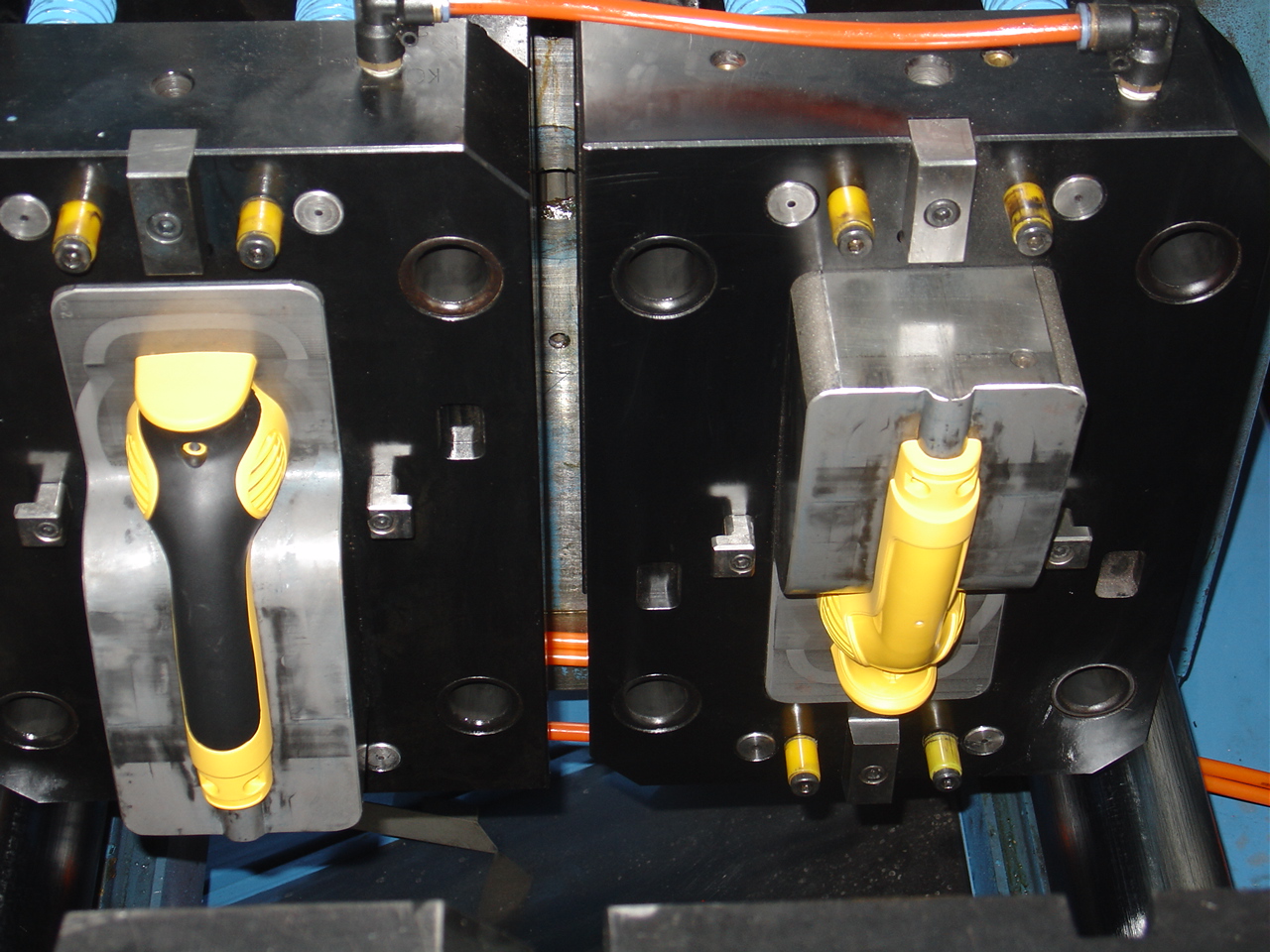
In this manufacturing process, you’ve got two different plastic compounds, one of which houses the circuitry and serves as a conductor and the other which serves as a simple housing. Once the circuitry is overlaid on top of the first plastic compound, the two housings are then joined to move through an electroless plating process. This final stage is where all of the plastic compounds with circuitry become metallized and ready for conducting current.

The one downside to the two-shot molding process is that its multiple parts make it hard to implement changes the further on in the design process you go. Because of this, you’ll commonly find MIDs manufactured with this technique that only includes simple circuitry and little changes planned for the lifetime of the product.
This manufacturing process does away with multiple plastic compounds and instead relies on the magic of lasers to add metal circuitry to a molded polymer. This process first starts with an injection molding to create the actual shape of the product. From there, the molding goes through a laser activation stage where wiring pattern get etched into the mold. And lastly, the molding goes through an electroless plating where the circuitry becomes metallized and conductive. Check out the video below to see this entire process in action:
https://www.youtube.com/watch?v=CAD6rRWFRn8
Once you’ve made your model with its conductive circuitry, you’ll then rely on a conventional pick and place machine to place all of the parts. For MID assemblies, manufacturers will typically rely on wire bonding, flip-chip mounting and conductive adhesive techniques to attach all of the requires SMD components and IC chips to a MID mold. And once all of the parts are attached, the housing heads through a reflow soldering machine to solder all of the parts.
It’s pretty clear that the world is moving towards increasing miniaturization of devices while still expecting to cram in a ton of advanced functionality. But how exactly are engineers going to be trained to think and design in this new three-dimensional perspective with MIDs? After all, many of us were raised to think in terms of 2D planes and flat surfaces when designing electronics.
This also brings into question another problem, how are we going to bring all of the engineering disciplines together to make this MID reality happen? Are we going to require different tools, maybe all with a unique interface but an underlying set of common data points and platforms? And more importantly, is this going to require a different way for us to collaborate and share our design data?
When MIDs come around, it’s no longer going to be a simple process of sending off your PCB to a mechanical designer and hoping it fits in an enclosure. Electrical and mechanical engineers won’t just be designing standalone pieces to products during their daily engineering. Instead, they’ll be designing an entire product, all at the same time!
The road ahead is still looking pretty fuzzy for how MIDs will gain momentum. There’s going to be a lot of changes needed, most importantly with how we work together as engineers. Who knows, maybe one day there won’t even be a separation between electrical and mechanical engineers. We could all one day find ourselves as electromechanical engineers. Only time will tell.
Ready to start thinking outside of the box with your designs? Try Autodesk EAGLE for free today!
By clicking subscribe, I agree to receive the Fusion newsletter and acknowledge the Autodesk Privacy Statement.
Success!
May we collect and use your data?
Learn more about the Third Party Services we use and our Privacy Statement.May we collect and use your data to tailor your experience?
Explore the benefits of a customized experience by managing your privacy settings for this site or visit our Privacy Statement to learn more about your options.