& Construction

Integrated BIM tools, including Revit, AutoCAD, and Civil 3D
& Manufacturing

Professional CAD/CAM tools built on Inventor and AutoCAD
12 min read
The Internet of Things (IoT) is here, it’s huge, and it’s only going to get more massive as time goes on. IoT has been described as the fourth Industrial Revolution. And if all the research and speculation is accurate from Gartner, we’re going to be seeing at least 26 billion devices connected to the internet by 2020. This is all great, but it’s easy to feel disconnected from the future-looking talk as a design engineer. After all, how much of a role are you really going to be playing in those fancy marketing words like Smart Homes, Smart Cars, and Smart Cities?
As it turns out, quite a lot. PCB designers all around the world probably have the hardest job of all when it comes to IoT, cramming in all of that advanced functionality into package sizes that just keep shrinking. So we’ve dug down into the practical details of the world of IoT, and here’s are the 10 things you’ll want to know to be a successful PCB designer in our connected future.
Gone are the days of having a ton of extra layout space to lay down all of your tracks, components, and vias. With IoT devices, you’ll be cramming in a ton of functionality into something that you can wear on your body, in your clothes, or even ingest in your body.
Take for example the Apple Watch. The aluminum model measures in at 38.6mm x 33.3mm with a depth of 11.4, all with a weight of only 28.2g. And while it might look beautiful on the outside, it’s also packing in a ton of functionality. You’ve got things like a LED display, memory, a SoC controller, a bunch of sensors, a Bluetooth chip, and a long-lasting battery. What you’ve got here is the functionality of something that would traditionally fit in the size of a smartphone, now being worn on your wrist.
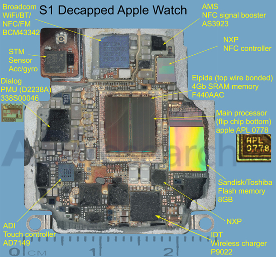
You can bet that the engineers at Apple were fighting for every inch of space on their board layout, and you can expect to do the same. Plan to cram in things like displays, cameras, microphones, sensors, charging ports, etc. all in a package that seems to shrink every year. To achieve all of this compact functionality and flexibility you’ll likely find yourself entering a whole new design domain that includes Rigid-Flex and High-Density Interconnect (HDI) PCBs.
HDIs are great as they allow for denser component placement and the use of blind, buried, and micro vias to save valuable board space. And as for Rigid-Flex PCBs, you can take advantage of all the bending and twisting to fit multiple PCBs into the smallest of enclosures. It is getting to a point where just ‘good enough’ PCBs will no longer be accepted by the market.
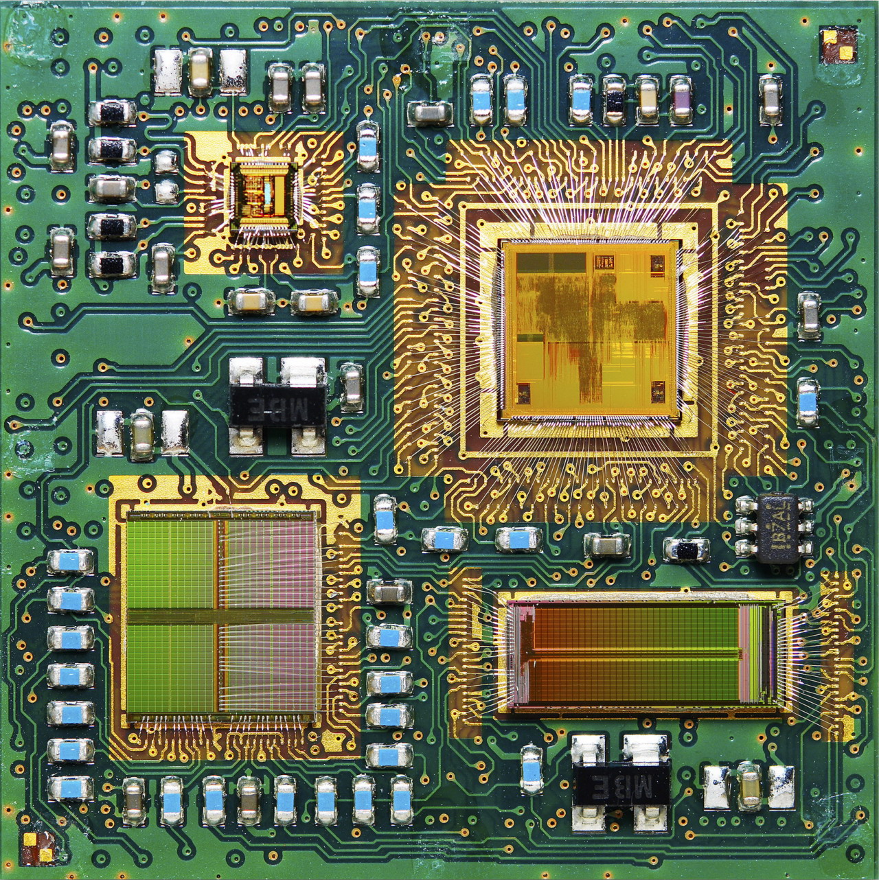
Say farewell to your traditional combination of through-hole and surface mount components. Today’s IoT devices are using some newer packaging technologies to keep things slim and thin, like:
We’re all likely used to designing a traditional circuit board and handing it off to our mechanical designer for a fit check. But in the world of IoT, this workflow won’t fly anymore. With smaller form factors, it’s going to be more important than ever to get every stakeholder on the same page at the beginning of the design process. All to ensure that both function, form, and business needs can come together smoothly.
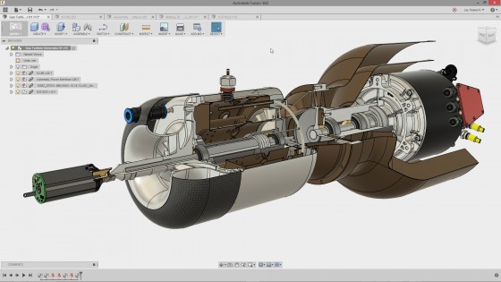
What does this mean for you as a PCB designer? Expect to do a lot more virtual prototyping to evaluate PCB size, the overall weight of your product, and your board’s fit within an enclosure before ever diving into the details of your circuitry. This focus on virtual prototyping will make it easy to focus on all aspects of the electronics design process, including 2D layout, 3D physical dimensions, and committing to your required list of BoM materials before you ever place a trace or component on your board.
Outside of the virtual prototyping and product planning process, you should also expect to spend some quality time bonding with your mechanical designer. It’s very likely that when IoT comes into full swing, you and your mechanical team will be designing your product in tandem. No more assembly lines.

This means that at every stage of the design journey, changes and modifications to both a mechanical assembly and circuit board are being shared between disciplines, in real time. Gone will be the days of doing the import/export dance to share component models and board outlines just to conduct a basic interference check. Instead, you’ll start to see ECAD and MCAD tools that bring engineers and their data closer together, all in one place, all in one tool.
This does raise some pretty significant concerns for the ECAD industry in particular. We’ve got a ton of PCB design tools out there that really don’t work well together, much less with MCAD software. With every tool using its own proprietary file format and data structure, we’ve got a long way to go to even get electrical engineers on the same page, much less electrical to mechanical.
If you think you’ve got time to reinvent the wheel now, just wait until you start developing IoT devices. Rather than focusing on reconstructing basic circuitry, you’ll start to see a movement in electronics design towards standardization.The reason for this comes down to efficiency and reliability. It’s just easier to reuse blocks of circuitry that have already been fully simulated and proven to work in the field. And you don’t have to re-design the same block of your schematic or layout over and over. The traditional schematic design process will become module design.
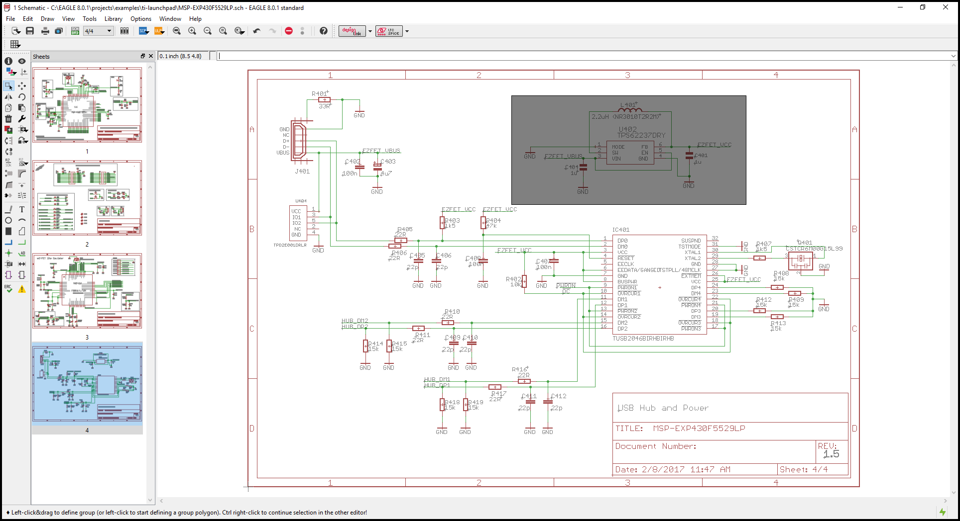
As your design process starts to move into IoT, expect to start saving and reusing modular schematics, part lists, and of course parts of your layout that have proven successful in part projects. Luckily you’ve already got the tools for the job in Autodesk EAGLE to make this happen. You are using Modular Design Blocks, right!?
The days of relying on traditional FR4 to have your square-shaped PCB manufactured might be over. In the age of IoT, circuitry needs to be flexible, and not only that, circuits will likely need to be embedded within other materials. Because of this, you’ll probably start to move away from FR4 in your IoT designs and into some new materials like plastic, flexi-rigid copper, and even mesh.
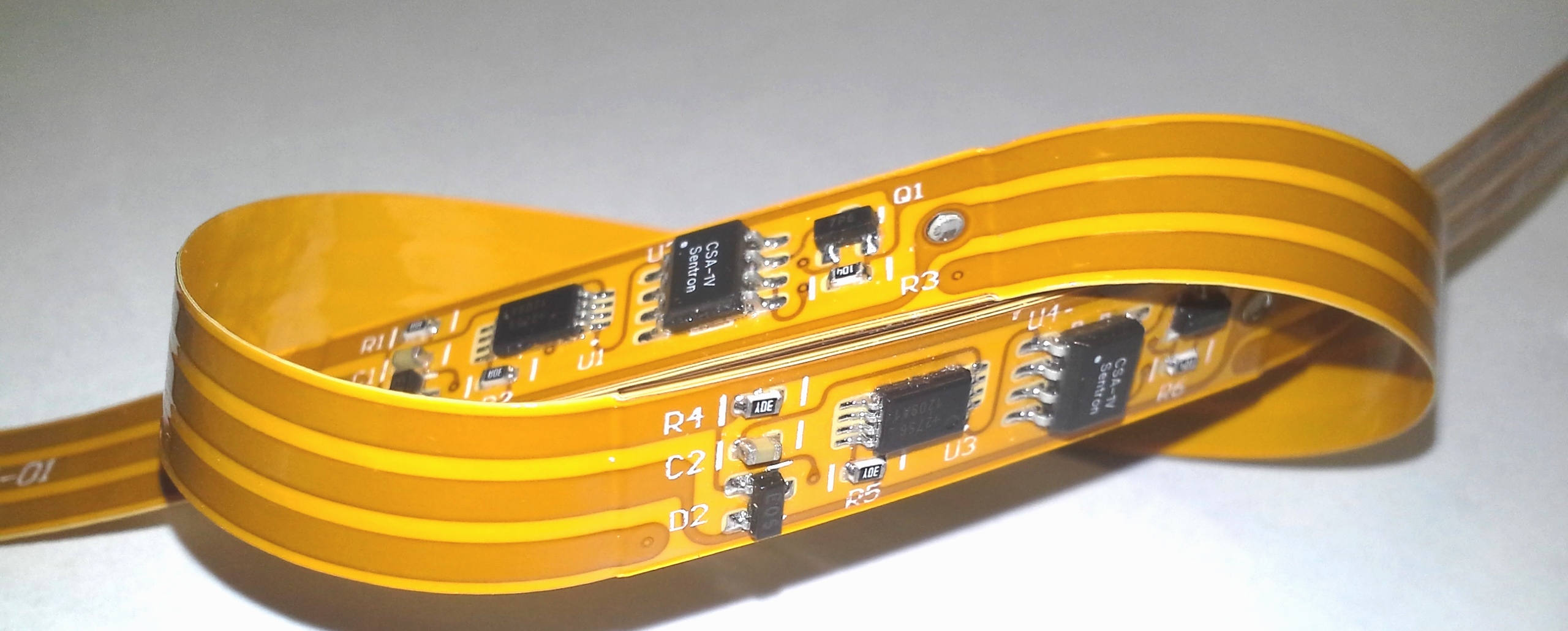
This is going to require help from specialists in the manufacturing and design realm that know the best way to design and work with these FR4 alternatives. If you’ve found yourself designing an IoT application that requires a new board material, be sure to seek out guidance first. If you don’t have anyone around to help you, then consider checking out these research firms that focus on wearable technologies and IoT for your information needs:
There’s little to no guarantee that the IoT product you’re designing will have a dedicated source of plug-in power. Most of these devices rely on batteries and even energy harvesting capabilities to keep them going throughout the day. Because of this, you’ll want to design your IoT product with a focus on efficient power consumption.
When planning power in your IoT design, you can strategize it regarding an allocated budget. Each functional circuit block on your PCB can be given its own power budget, which will give you a lot more flexibility than just considering power consumption for the product as a whole. Chances are you can also talk to a component supplier if you’re running into power consumption problems. They might have suggestions for alternative parts that can keep you within your power budget.
Once you have your power consumption all planned out, you’ll also need to verify and test each power state of your PCB as it cycles through various tasks. Be ready to do some validation for sending, standby, Rx/TX, etc. and seeing how those impact your battery usage.
Wireless connectivity is a core foundation of any IoT product, allowing a device to sense its surroundings, collect data, and send it off to the cloud for interpretation. All of this is made possible through a variety of wireless modules and RF circuits, but how are you going to find room for all of them?
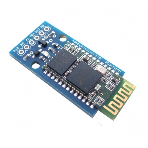
These days there’s a ton of off-the-shelf modules and RF components that are designed for IoT and wearable products. These parts keep their footprints as small as possible while still including all the functionality you need. What wireless module and protocol you decide to use in your PCB will ultimately boil down to several factors, including required range, data transfer speeds, security requirements, and power consumption. Chances are you’ll be using one or many of these protocols to get the job done:
As you might imagine, this list is by no means exhaustive. There are a ton of other IoT protocols out there, and plenty more in development as the needs of our connected future changes. We do wonder, will there ever be one wireless protocol to rule the future of IoT? Probably not. With every device having different needs in power consumption, range, and data transfer, you’ll likely always find yourself mixing and matching protocols and modules depending on your requirements.
Here’s the problem with the human body, it’s extremely lossy. This can spell bad business for maintaining a strong signal when transmitting data. Working on a smartwatch that has an antenna? You’ll need a way to get those electromagnetic fields as far away from the body as possible. This might require some specialist knowledge, and also the use of components like low-noise amplifiers.
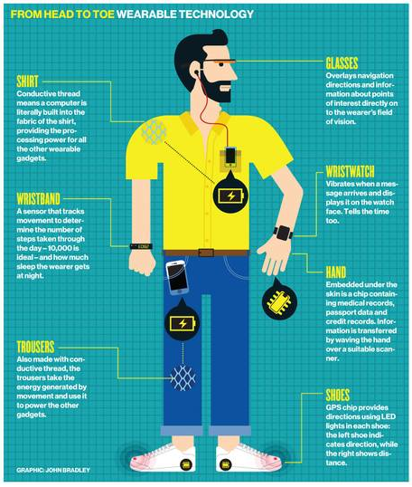
In addition to the radiation issues with the body, there’s also the matter of humidity. As we all know moisture can completely destroy a working circuit. And when you start designing high-impedance circuits in a wearable, moisture from a body contacting a circuit can spell disaster if not planned for correctly.
Ideally, this will be a problem that your mechanical engineer can assist with by designing a package that is fully sealed to provide humidity resistance for your PCB. But if that’s not possible, there’s also the option of applying a conformal coating to your board, which can help to stop moisture from penetrating into sensitive components.
It’s one thing to swap out a fried through-hole component on a circuit board, and quite another to do the same thing on a miniaturized IoT device. Someone strapping a smartwatch to their wrist or a hearing aid into their ear simply won’t have the tolerance for failure with your device. It will just need to work, all the time.
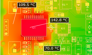
As a PCB designer, this means you’ll be spending a lot more time in simulations programs such as PSpice, carefully optimizing your prototype for ideal performance. You’ll also be paying a lot more attention to thermal management. With multiple sensors, sensitive components, and multiple boards stacked in the same space, proper cooling can become a huge problem. Can a change in temperature affect how your components will function? That’s something you’ll want to know.
It’s pretty clear that electronics design as a whole is going to go through some serious changes in the future to deal with the needs of IoT. And while everything you learned in your EE studies or hobbyist tinkering will still be applicable, there’s just going to be a lot more details to deal with. Is your power consumption in check? What kind of heat is your board throwing off? And what protocol are you going to use? These are all questions that you’ll have to answer.
In the age of IoT, the name of the engineering game is going to be all about efficiency, reliability, and collaboration. You aren’t just designing circuit boards anymore; you’re developing products. And this definitely isn’t your typical PCB design process anymore.
Do your tools have what it takes to design the next IoT product? Subscribe to Autodesk EAGLE today!
By clicking subscribe, I agree to receive the Fusion newsletter and acknowledge the Autodesk Privacy Statement.
Success!
May we collect and use your data?
Learn more about the Third Party Services we use and our Privacy Statement.May we collect and use your data to tailor your experience?
Explore the benefits of a customized experience by managing your privacy settings for this site or visit our Privacy Statement to learn more about your options.