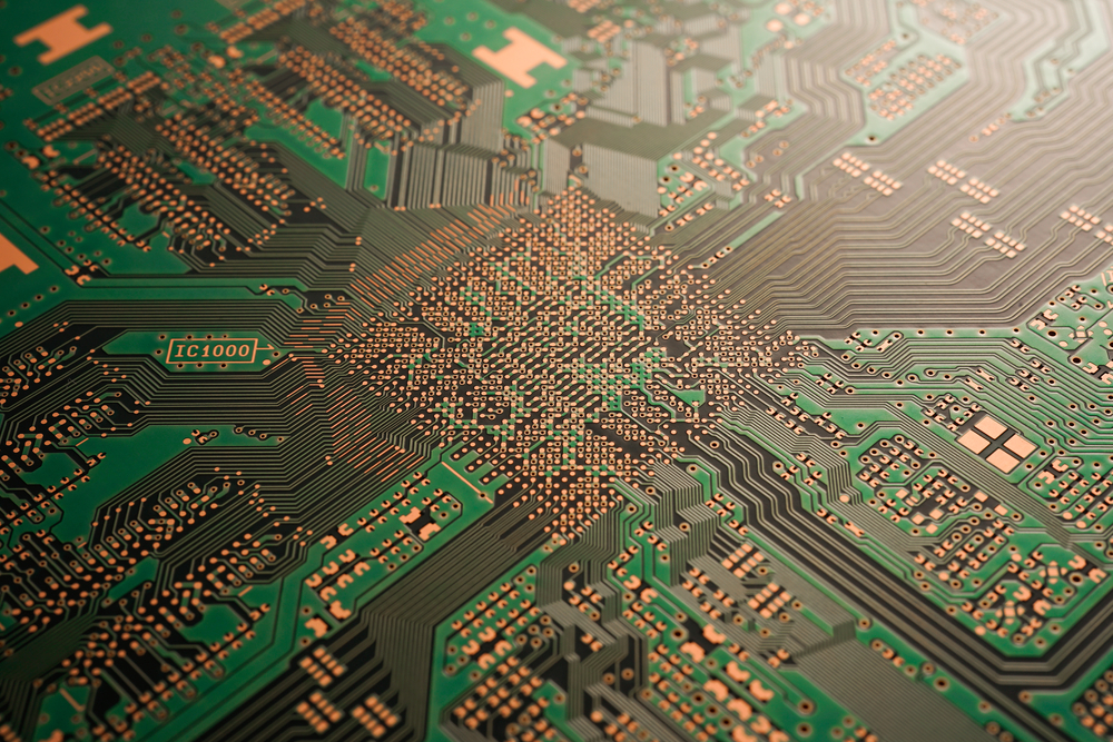
Physics, for some, may have been just one of a slew of too-early classes in college, but in the world of engineering, physics is everything. For many PCB designers, physics is essential to creating a board that functions appropriately in the real world – a world in which weather, environment, and humans can mean big (and unexpected) changes. Understanding the behavior of electronics relies heavily on physics because outside influences have a significant impact on how things operate.
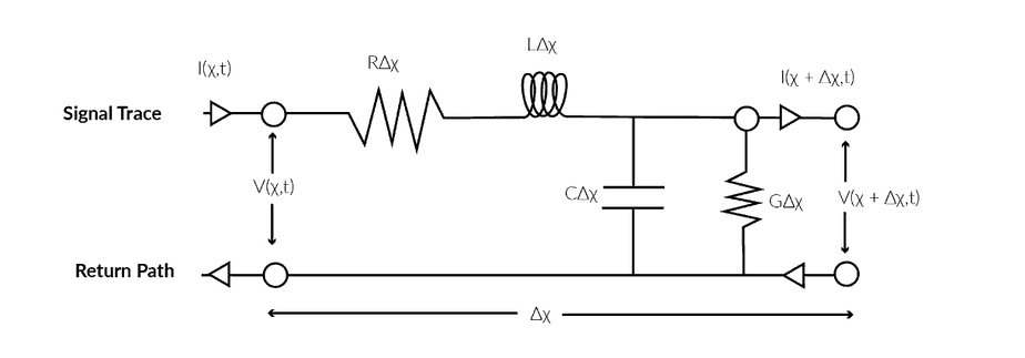
Transmission line segment. Image credit.
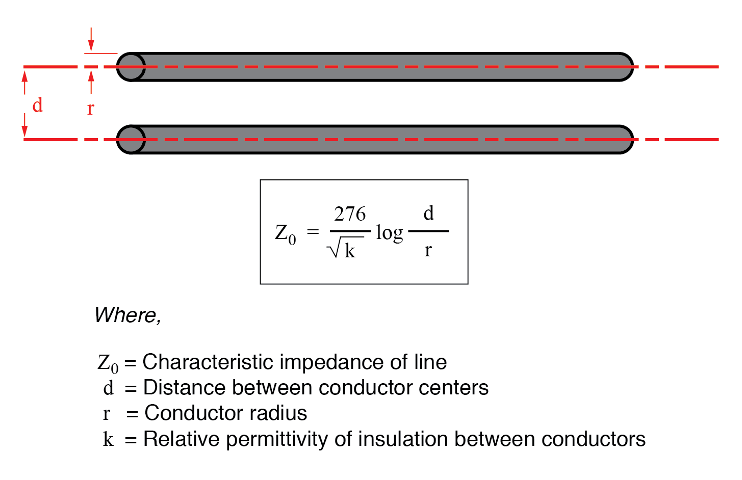
If a PCB trace is at a short distance and operating at a low frequency, it may be an ideal connection (zero-ohm resistor). There is no space in which resistance, capacitance, or inductance may occur to change the behavior. As the signal trace lengthens compared to the frequency of the signal, the signal trace becomes a transmission line. As speed increases, a short PCB trace also becomes a transmission line. Transmission lines operate at a high frequency in which the AC creates an always-present resistance, capacitance, and inductance on the trace. Together, these are called characteristic impedance.
Reflection Perfection

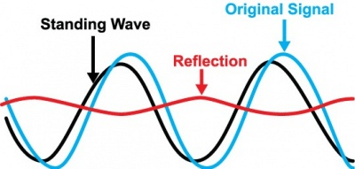
When the load impedance on a line matches the characteristic impedance, it has the same effect as an infinitely long transmission line. All of the energy is absorbed, which prevents reflections – think about going to the waterpark. In a pool, you could create a wave that would, upon reaching a wall, reflect and come back to you. In an infinity pool, however, it cannot reflect. This is the same idea.
An electrical circuit with an impedance mismatch will allow for a partial reflection – the pool in our example essentially sends a piece back. If the source impedance isn’t matched to the line, the reflection goes back and forth, and energy is lost a little bit at a time. Eventually, all of the energy has been used. In a line, reflections disrupt the signal, which can lead to problems with data, among other things.
Wait for the Crosstalk
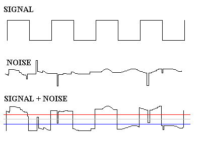
Too much noise will affect your signals—Image Source.
On a PCB, there are electrical traces that run parallel to one another with very little space in between. In close proximity and at high speeds, this produces a mutual capacitance, causing energy to transfer from one trace to another. There is also a magnetic field at high speeds, which creates a smaller magnetic field opposite to the first on traces that run alongside one another and are close together. The energy, coupled as the result of mutual capacitance and mutual inductance, is called crosstalk. To minimize it, engineers can increase the spaces between nets, shorten the parallel trace segments, use ground planes for the return paths to decrease the characteristic impedance of the signal traces, and utilize differential pairs.
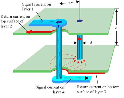
Vias can get your traces from source to sink on high-speed layouts. Image Source.
Fusion 360: Preventing Problems Before They Happen
Once you understand the basics of transmission lines and how outside forces might impact them, you can ensure that your designs take external factors into account. The Fusion 360 electronics workspace ensures that you’re able to allow adequate clearances and coupling from the get-go or make adjustments at any point in the process to allow for maximum efficiency. With an easy-to-use schematic editor and robust library support, Fusion 360 is committed to helping you overcome design roadblocks so that you excel!
Try PCB design and Electronics in Fusion 360 today!
