Don’t Get Zapped! What You Need to Know About ESD, and How to Design For It
Ever wish you were like Zeus, capable of wielding the power of electric energy to smite your enemies? Worry not, we’ve got just what you need, Electrostatic Discharge (ESD)! Now you can teach those pesky capacitors and ICs who’s boss, and heck, even entire circuit boards, are at your mercy.
All jokes aside, there has never been a period in electronics design when ESD has been more of a problem. With ICs getting smaller every year, and devices becoming more advanced, the chance for ESD to wreak havoc on your design is a huge concern. As a designer using these devices, it’s no longer just about whipping out the anti-static mats and wrist straps; now you need to double down on adding ESD protection at design time, not after. But what do you need to include? Let’s find out.
What is Electrostatic Discharge?
Electrostatic Discharge (ESD) is the spontaneous and often unintended flow of electricity between two objects that have come in contact with each other. That might not be a physical contact; even close proximity will get that current jumping.
ESD isn’t a new problem. In the 1400s European and Caribbean military forts were implementing safety nets to prevent ESD from blowing up their gunpowder storage. And in 1860, paper mills throughout the United States were taking advantage of steam drums, flame ionization, and grounding techniques to keep static electricity out of their paper drying process.
As you can see, ESD isn’t just a problem that plagues electronics. You’ll find this natural phenomenon affecting a variety of industries from petrochemical, pharmaceutical, agriculture, textiles, plastics, and a whole lot more. But closer to home in electronics design, the consequences of ESD can be catastrophic, including:
- Wrecking production. Having unintentionally ESD that enters the manufacturing process can affect the production of products including both their quality and reliability. There’s nothing worse than a manufacturer having to scrap an entire circuit board run because ESD entered the mix.
- Damaging components. ESD can also damage components on a circuit board, whether that’s during production or once you have that PCB in your hand. While some parts are tough enough to handle ESD, others like ICs and semiconductors are permanently damaged by just the smallest jump in current.
- Disrupting electronic equipment. Even when ESD doesn’t wipe out a circuit board immediately, it can eventually cripple sensitive electronic equipment weeks or months down the road if the problem goes unnoticed. This can be a huge problem for military and medical applications that have a need for reliability.
How ESD Works
At the heart of ESD is a simple principle of electrostatic charge, which builds when two materials come into contact and separate from one another. You’re probably familiar with the most common form of electrostatic charge, like when you rub your feet against the floor while wearing socks and get a shock when touching a doorknob. This process of a continuous contact/separation between two materials all starts at the atomic level.
When two materials touch, what’s going on behind the scenes is a transfer of electrons. While atoms in a balanced state have an equal number of electrons(-) and protons(+), when these electrons begin to transfer between materials through continual and consistent contact, then everything gets out of balance. Take for example the images below; here we can see that two identical atoms that have come into contact and separated through the process of triboelectric charge. Now Material B has more electrons than Material A, and there’s an imbalance to the whole equation. How will it find equilibrium?
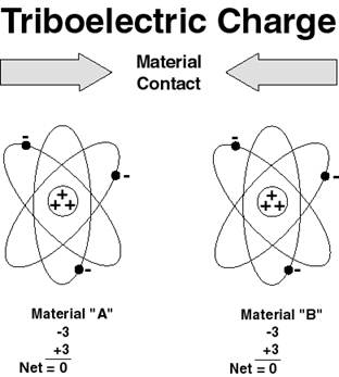
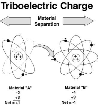
At their core, atoms will always seek balance. And so what happens when you run your socks across the floor, collecting excess electrons in the process? Those electrons are going to find the path of least resistance in a nearby object to find equilibrium. And if that object is a metal doorknob (an excellent conductor), then you’ll get a shock in the process as those electrons transfer.

The amount of charge that gets created by this triboelectric charging process has many variables to take into account, including:
- The size of the contact materials
- The speed at which two materials separate
- The relative humidity of the environment the materials are in
- The chemical makeup of the materials making contact
You can measure the electric charge that you create between two materials in coulombs, with the following equation:
q = CV
Here, q is the charge of an object, which is determined by multiplying its capacitance, C, with the voltage potential of the object, V. When measuring the effects of ESD on a component or circuit board, you’ll commonly see ESD being described in terms of voltage or current.
Types of ESD
Not all ESD is created the same. While this natural phenomenon might disrupt the workings of your components or circuit board, how it goes about doing so can be a little mysterious. Typically when you have an ESD issue, you’ll find out in one of two ways:
Catastrophic Failure
This is the most obvious, where your entire circuit board or a particular component on your PCB immediately stops working. ESD will typically cause the metal to melt, oxide failure, or a junction breakdown in those ultra sensitive parts like semiconductors and integrated circuits. More often than not, catastrophic ESD failures will be found immediately when the device is tested.

Latent Defect
Things get a little more tricky when ESD affects a circuit board or component but doesn’t completely disable it. In the Latent Defect situation, an electrostatic discharge will occur, causing a part to become degraded, yet still functional. But for how much longer is the major issue. You might find yourself shipping a product or system with ESD-degraded devices, only to find them failing in the field weeks or months down the road. These are the most costly forms of ESD to fix.
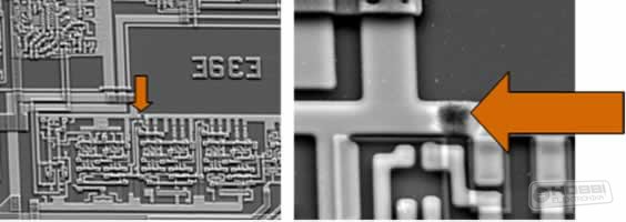
Whether ESD is crippling an entire circuit board all at once, or just putting a dent in a circuit for problems down the road, there are a number of ways this damage can happen. When ESD does discharge energy, it will occur in one of three ways:
- Discharging to a device. In this situation, a charged conductor will discharge to another object, like from your body to an electronic component. Something as simple as touching the leads on an IC with your finger can easily cause ESD damage.
- Discharging from a device. In this situation, ESD is discharged from an electrically sensitive device. This most commonly happens when an electric charge is built up in the device through constant contact/separation with packaging materials or machinery in an automated assembly process.
- Discharging through field induction. This situation is caused when a device comes into contact with the electrostatic field created from an ESD. Just placing a sensitive electronic component in this field is enough to disable it for good.
Is Your Device Susceptible to ESD?
Not all electronic devices or components are sensitive to ESD, and those that can withstand the zap have a relatively high resolve for withstanding voltage spikes. However, more sensitive components like integrated circuits and microprocessors typically can only withstand 100V, and some can barely handle 10V. The smaller that package sizes, the more sensitive the device.
To stay ESD aware, here’s a quick list of some of the most sensitive electronic devices in use that is susceptible to damage:
- Microwave devices like Schottky barrier diodes and point contact diodes
- Discrete MOSFET devices
- Junction field effect transistors (JFETs)
- Charged coupled devices (CCDs)
- Precision voltage regulator diodes
- Operational amplifiers (Op Amps)
- Thin film resistors
- Integrated circuits
- Very high speed integrated circuits (VHSIC)
- Laser diodes
- Silicon controlled rectifiers (SCRs)
How to Design for ESD Protection
Now that you’ve got a solid background on what ESD is all about let’s talk about what you can do about it. It’s not just about protecting yourself from ESD while tinkering with electronic devices with an anti-static mat and wrist straps. Way before you ever get a board back from your manufacturer, you need to be taking steps to add ESD protection into your design process. Let’s dive deeper:
The overall goal of designing ESD protection into your PCB is straightforward – prevent voltage levels from rising to a point where they’ll start to damage your interface devices. Check out the image below. This is a typical simulated response curve for an electrostatic discharge as defined by IEC61000-4-5. This graph shows a peak voltage between 2,000 and 8000V, with a rise time of approximately 1ns and a peak current level at 30A.
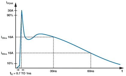
Now, keeping these figures in mind, consider some of today’s modern chipsets and integrated circuits. These devices rarely tolerate DC voltages over 3.3V, so an electrostatic discharge means immediate death for these mission-critical parts.
When you put this problem in perspective, there are a ton of variables to consider in both the circuit design and board layout process to ensure that your device is properly protected against ESD. This problem becomes especially pronounced at the board layout level when considering the ill effects of parasitic inductance. Take for example this equation:
VL, parasitic = Lparasitic × di/dt
This will get you the voltage calculation for your parasitic inductance. Here, Lparasitic is the parasitic inductance of the trace, and VLparasitic is the voltage developed across it after a change in current over the change in time, di/dt.
Using this equation, if you send an 8-kV, 30A ESD charge through a PCB trace with just 1-nH inductance, this will generate a 30V spike on a trace, but to what is that trace connected? If it’s an IC, you can guarantee that component is getting fried.
We think you get the idea now, ESD is no joke! So here’s what you can do about it.
Circuit Design Protection
When designing your circuit, consider adding a basic transient voltage suppressor (TVS) at your input. This protective circuit consists of two diodes and an avalanche diode, which works together to reduce the change of an ESD destroying your components. The way a TVS works is pretty simple:
- Both diodes are reverse biased under normal operating conditions
- If an ESD pulse occurs and raises the input voltage above the rail voltage, the first diode will conduct
- If the voltage falls below the ground voltage, then the second diode will conduct
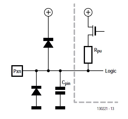
Put together, this circuit will effectively “clamp” the voltage to within an established range, and can be approximated by the following equation:
Vclamp = Vconduction + (Rdynamic x current)
Here, the total clamped voltage, Vclamp, is related to the conduction, Vconduction, of the type of diode being used and the dynamic resistance of the diode, Rdynamic x current. Keep in mind, even with this protective circuit in place using 5V DC clamp voltages and fast switching diodes; you’ll still likely see ESD spikes over 100V. But the good news is that the protective circuit will limit the discharge to a shorter duration so your circuit can survive the aftermath.
Board Layout Protection
When it comes to keeping your circuit board protected from unintended ESD attacks, keep the following tips in mind:
- Remember your trace lengths
Always keep the traces connecting to an ESD connector as short as possible. How short? Consider this – lengthening an ESD protector trace away from its device from 200 mils to 400 mils can increase voltages by 75%. Sometimes there’s nothing you can do about this, maybe the way your board layout is organized keeps an ESD device from being positioned directly on a PCB trace. But the farther away you place the ESD part from the trace, the more of a voltage spike you’ll be risking.
The same holds true for ground buses. In some designs, the ESD device’s ground might have to pass through vias and take a roundabout path to finally reach its ground plane. But doing this will again lead to some serious spikes in voltage, so keep those traces connecting ESD devices as short as possible.
- Watch out for circuit loops
Always take the time to review your design to ensure you have no loops on your layout. This can help significantly with ESD protection because spikes in current and voltage are easily induced in any kind of loop. Also make sure to use multiple ground planes if possible, which will help your signals to be grounded effectively and reduce the possibility of ground loops.
- Route away from the edge
The closer your traces are to the edge of your board, the more likely they are to pick up electrostatic discharges. Always try to keep any sensitive traces 50 mils away from the edge of your board. Of course, input and output lines will need to find their way to the edge at some point, but these can be immediately routed away to minimize ESD dangers. However, do check with your manufacturer for their recommended clearances.
- Keep component interconnections together
There’s a good reason to keep components with shared interconnections together – the longer the traces, the more they act like antennas. Those antennas can easily receive emissions from ESD pulses. Be sure to place all of your components with shared interconnections close together, which will help to reduce antenna-like effects while also keeping your board organized.
- Stay away from your TVS circuit
Lastly, we always recommend keeping unprotected circuits away from the traces between a TVS circuit and its input. Doing this will allow you to minimize the exposure of sensitive components from any kind of field induction. Also be sure to place parts that are on a sensitive line closer to the center of your board to balance the parasitic inductance of your circuit.
These ESD protection tips are by no means exhaustive, and there’s a ton of other strategies you can implement to keep your PCB protected. Be sure to check out this great ESD Protection Layout Guide by Texas Instruments for a deeper dive.
Don’t Get Zapped
As our electronic devices keep getting smaller and more advanced, the risks for ESD damage continue to increase. But not all ESD damage can be seen immediately, with latent defects on mission critical components cropping up weeks, months, or maybe even years down the road. As an engineer, it’s up to you to design ESD protection into your circuit and board layout. So plug in that TVS circuit, keep those trace lengths short and away from your board edge, and keep those circuits together. With all of these tips in hand, you’ll be well on your way toward designing a PCB that’s protected from ESD right the first time.
Don’t get zapped! Design your next PCB with our ESD protection tips in mind with Autodesk EAGLE. Try it for free today!
