Every Layer in Autodesk EAGLE and What You Need to Know About Them
If you’ve ever looked at the layers list in Autodesk EAGLE and felt entirely overwhelmed, then this blog post is for you! Layers are a critical component of your PCB design, allowing you to organize a ton of information without cluttering your view. And when you’re ready to generate documentation to share with your manufacturer, your Gerbers will be pulling data directly from many of these layers to communicate your design intent clearly. The problem is, there are 38 layers to know about (52 if you have EAGLE Premium), and remembering what they’re all used for can be a challenge. Worry not though, below you’ll find a complete list of every layer in Autodesk EAGLE, and what you need to know about them.
Layer 1: Top
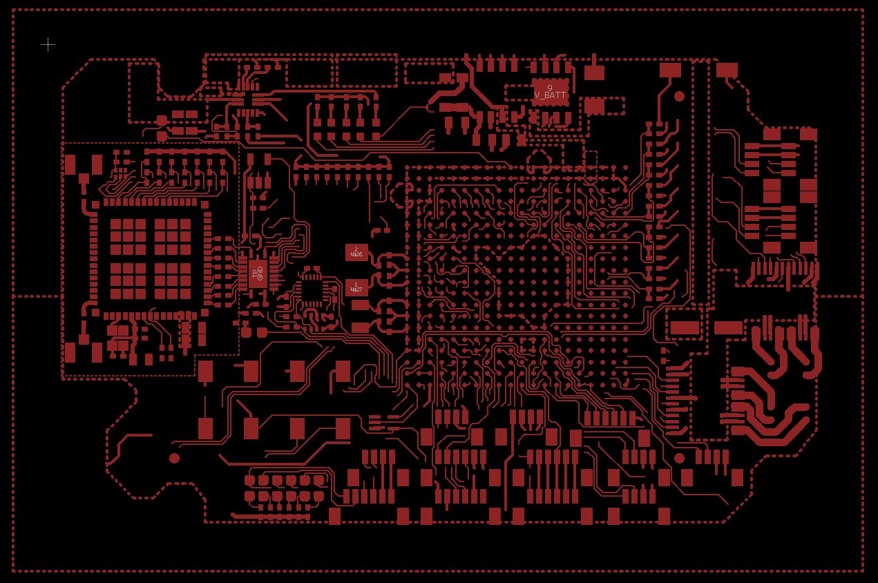
This first layer contains the copper on the top of your board, whether that’s a polygon from a copper pour or individual copper traces. Using this layer to generate a pour will provide an accessible area of copper for all of your signals to ground. Also, when creating pads for surface mount components, Autodesk EAGLE will default to using Layer 1 for the pad’s placement.
Layer 2-15: Route
If you don’t see these layers listed in your Visible Layers dialog. 2-15 are reserved for those with a Premium EAGLE Subscription and offer a ton of inner layers to route on for multilayer PCBs. To use these layers for Premium Subscribers, you’ll need to modify your layer stackup via Tools » DRC » Layers tab.
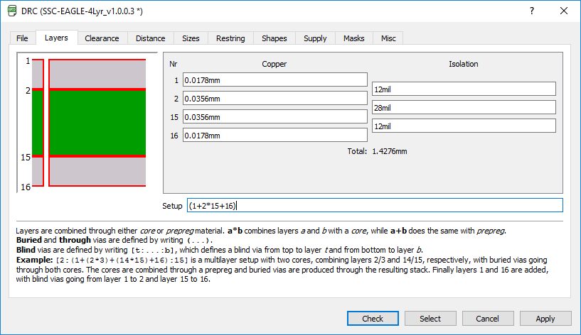
If you’re planning to design a multilayer PCB then how your top/bottom and middle layers are organized will be slightly different than you’d expect. For example, creating a 4 layer board won’t just use layers 1, 2, 3, and 4. Rather, EAGLE will use Layer 1 (top), 2, 15, and 16 (bottom) to bring it all together.
Layer 16: Bottom
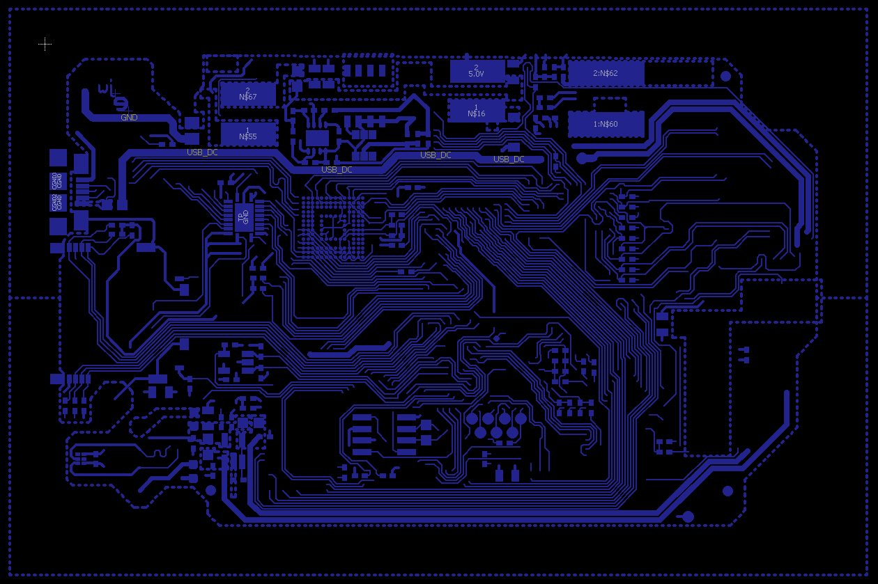
Just like Layer 1, this layer contains the copper on the bottom of your board, whether that’s from copper pours or individual copper traces. Components placed on the bottom of your board will also have their pads placed here.
Layer 17: Pads
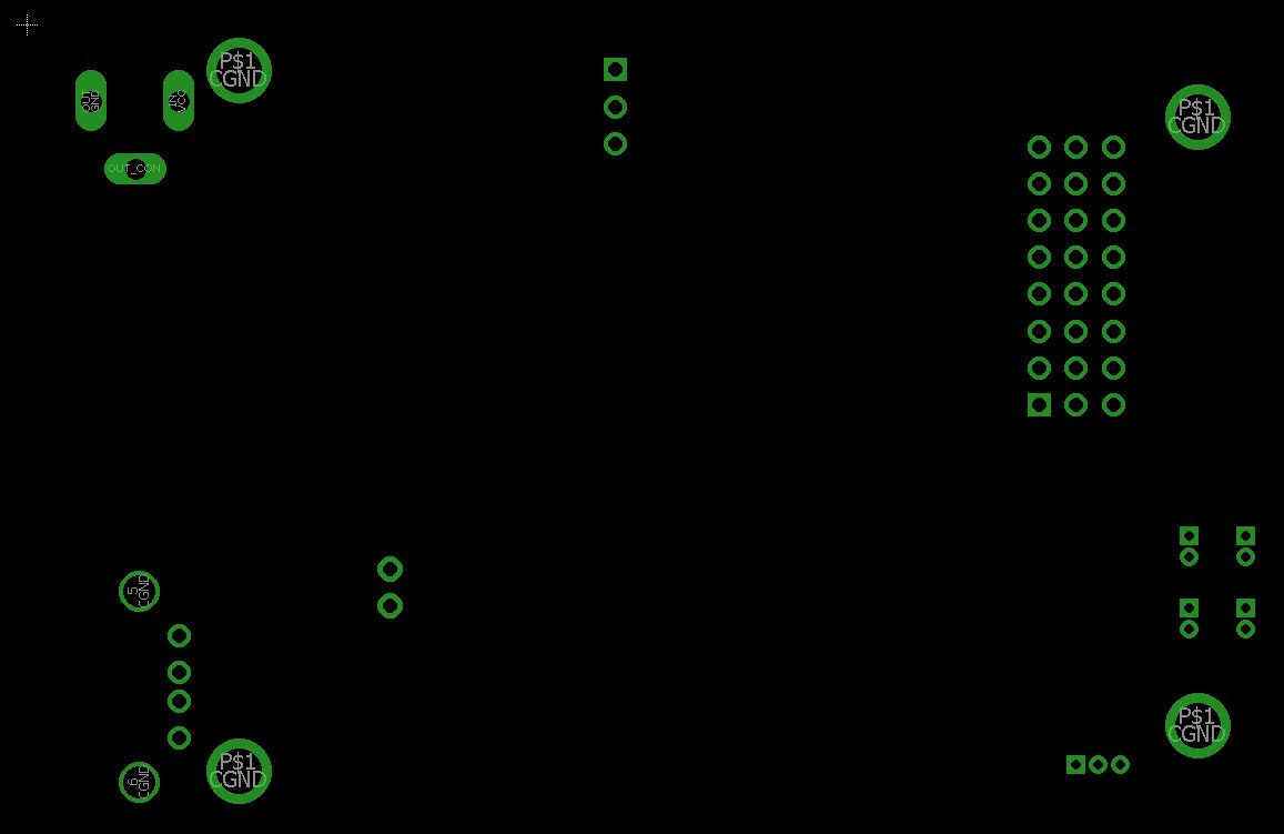
Here you’ll find all of your through-hole pads, which includes both the hole on the copper surrounding it (Annular Ring). When placing a pad on this layer, it will place an annular ring on both the top and bottom layers of your board. Keep in mind that you’ll rarely need to tinker with this layer, as through-hole pads are automatically generated once you place down a through-hole package.
Layer 18: Vias
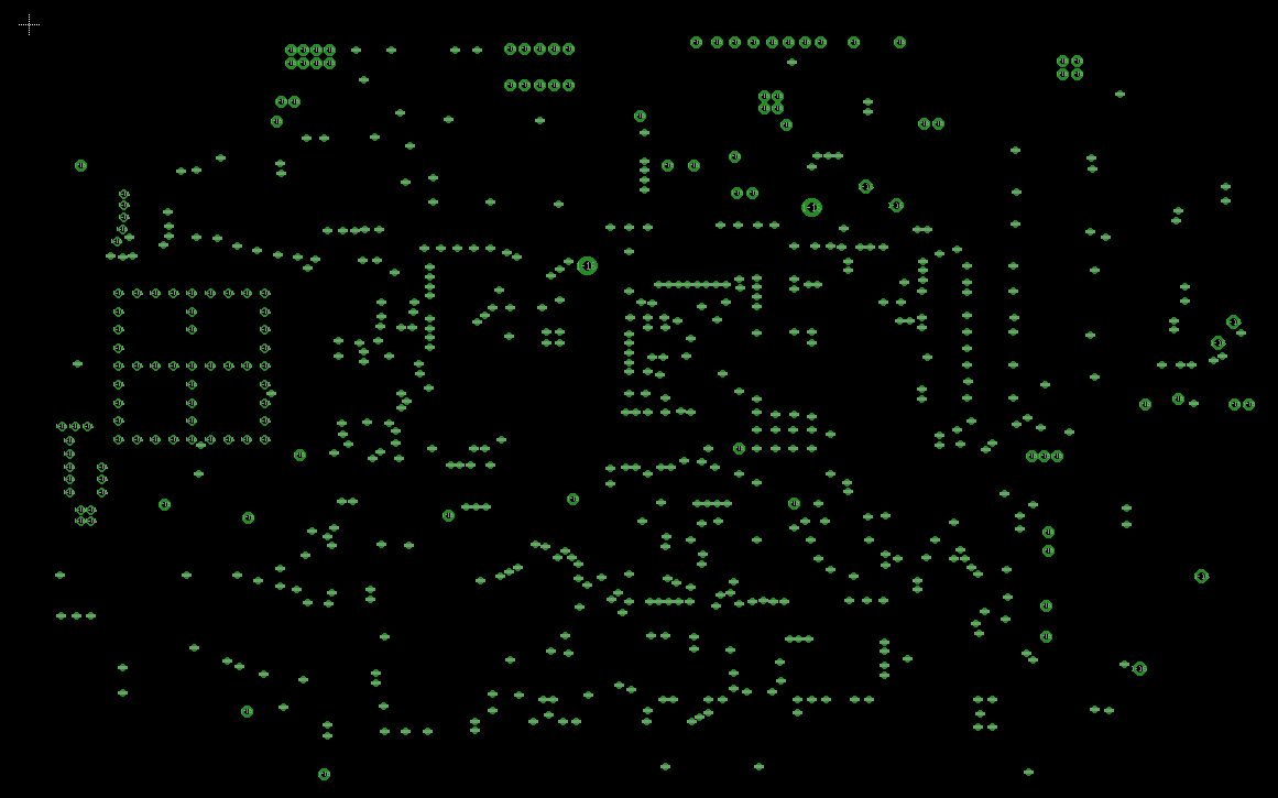
This is the layer for all of your vias, which provide a quick path of connectivity for signals between layers on your PCB. Note that both vias and through-hole pads will look nearly identical, so it’s always useful to be able to hide/show just Layer 18 or 17 to understand what specific object you’re viewing.
Layer 19: Unrouted
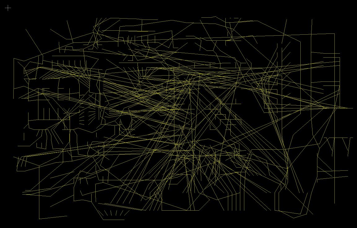
When you first start a PCB layout, all of your components will be connected with a set of airwires, also called a ratsnest. These lines specify connectivity between all of the pins on your components, and these lines live on the Unrouted layer until they get connected. By the time your PCB has been fully routed, you should no longer have any visible Unrouted wires.
Layer 20: Dimension
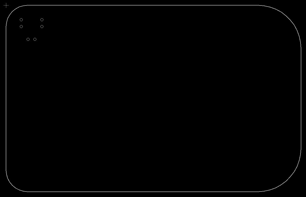
The Dimension layer has several purposes, the first of which is to specify the outline of your board. Secondarily, you can also use this layer in your design rules to keep copper pours away from the edge of your PCB.
Some fab houses like OSH Park will use this Dimension layer to generate a board outline Gerber. This will serve as the exact shape of your PCB when they cut it into a fabrication panel.
Layer 21-22: tPlace/bPlace
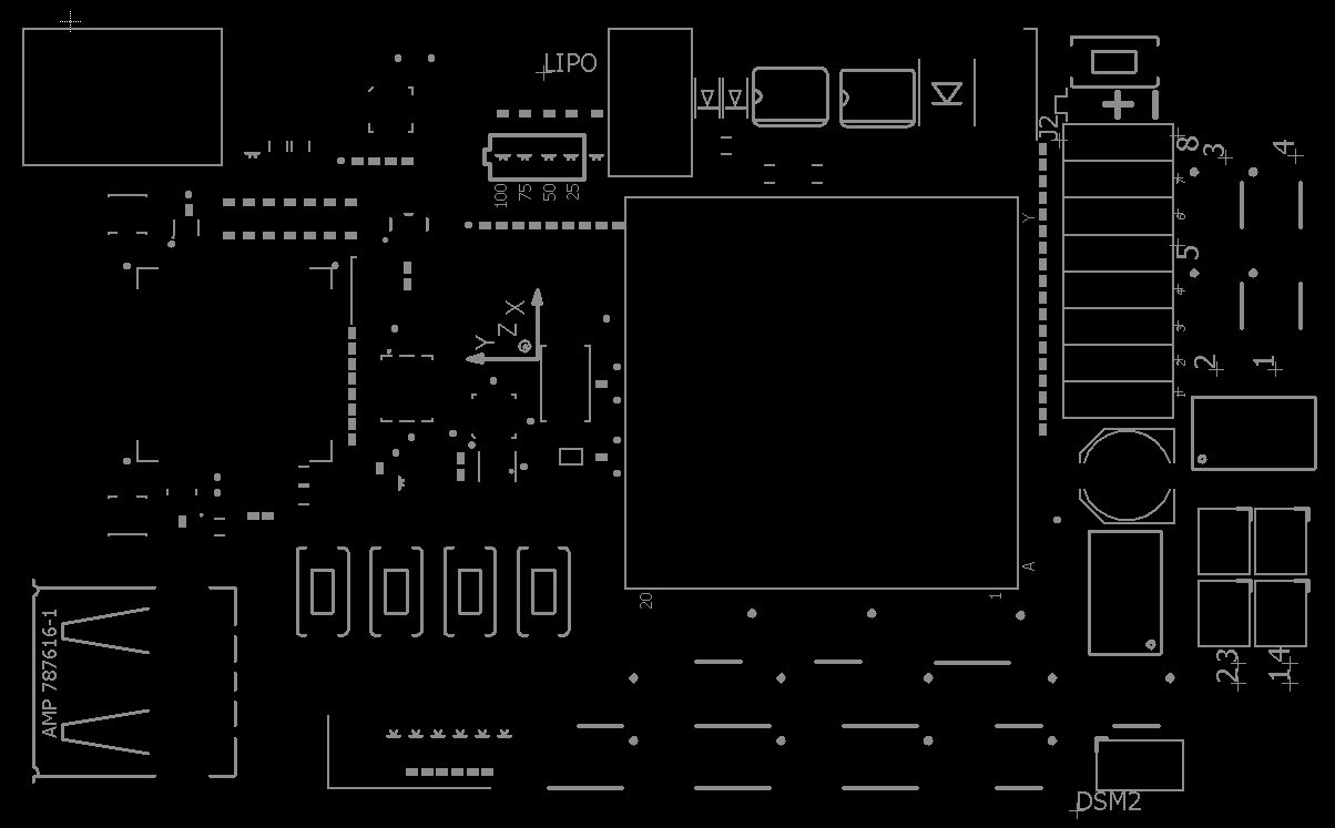
These two layers contain both the top and bottom silkscreen on your PCB, and also component outlines to show the positioning of parts. You need to be careful when using this layer not to place silkscreen on any soldered areas. Otherwise, you could risk creating a short on your board or creating a unsolderable pad.
As an alternative to these layers, consider placing additional silkscreen on Layer 51: tDocu for your own personal reference. This layer won’t be included in your manufacturing data or printed on your PCB so that you can include a lot more details. However, if you want to add any kind of additional artwork outside of regular silkscreen, like text or logos, then Layer 21-22 is the place to do it.
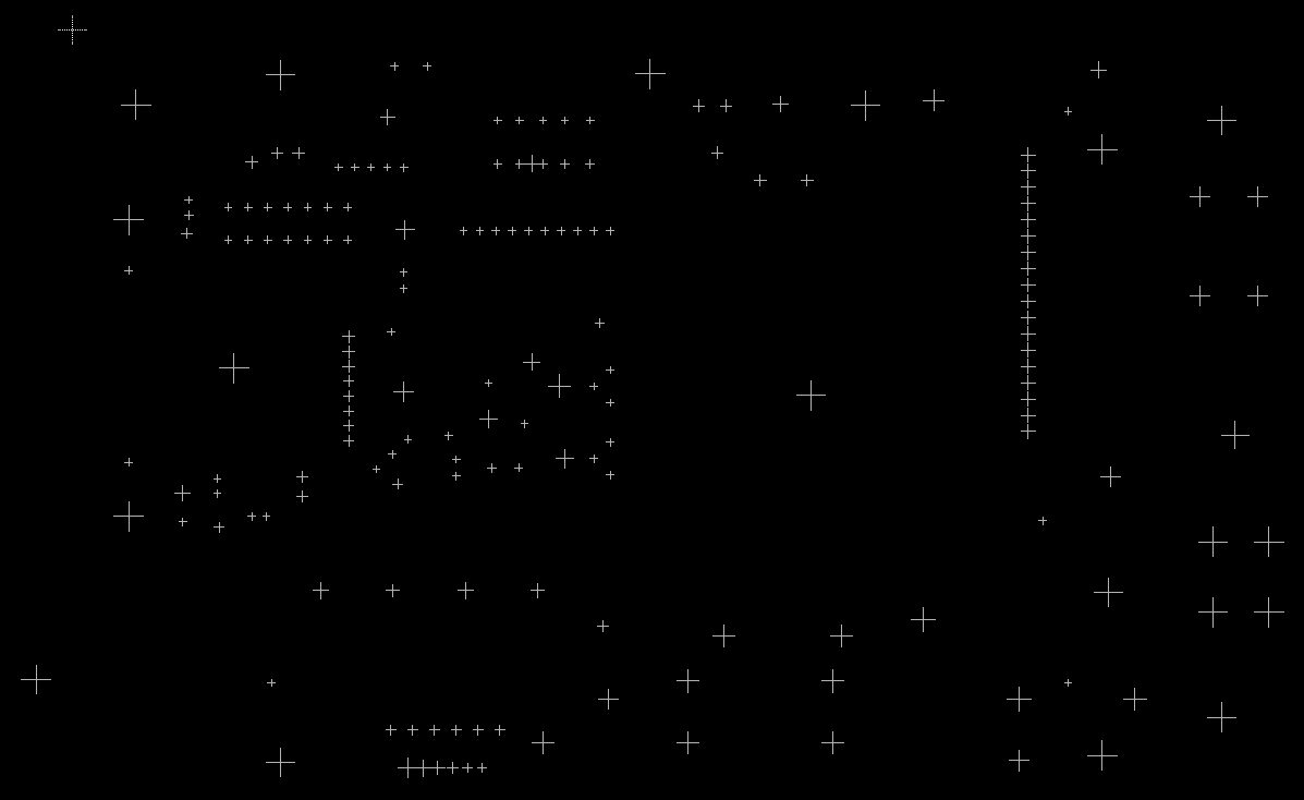
Layer 23-24: tOrigins/bOrigins
These two layers contain both the top and bottom sides of your component origins. If you isolate to show only this layer in EAGLE, you’ll see a bunch of crosses in the middle of where each of your components used to be. This is the origin point.
You might want to consider turning this layer off by default if you need to keep your components locked in place. Without a visible origin point, you won’t be able to move your components, and you can focus on other aspects of your board layout.
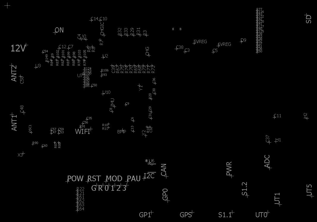
Layer 25-26: tNames/bNames
As the name suggests, these two layers contain both the top and bottom print for your component names. Every component on your PCB has a unique name, also called a reference designator, and will look something like R1, C1, D1, etc.
You won’t need to worry about your component names as they will be automatically generated when you place a part. However, it can be helpful to arrange the names all in the same orientation to make your board easier to read and reference.
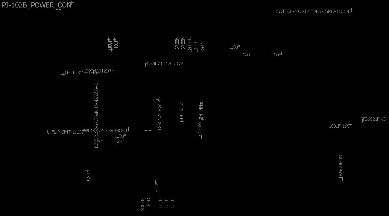
Layer 27-28: tValues/bValues
Again as the name suggests, these two layers contain the specific values for every component on your board. For example, a resistor will have its specific resistance listed, maybe as 10K. Or for a capacitor, you’ll see the capacitance listed, maybe as 0.1uF.
Many designers choose not to include this layer on their physical PCB, opting instead to have a Bill of Materials (BOM) that they can reference by looking up the reference designator of a particular component. However, if you’re planning to design a PCB for a kit or hand-assembled board, then it’s super helpful to list both the component names and values on your PCB. This will make the assembly process a lot easier to digest.
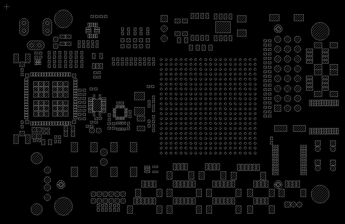
Layer 29-30: tStop/bStop
These two layers indicate where your solder mask should not be applied. When placing either through-hole or surface mount components, these parts will typically include a solder mask expansion area that resides on these two layers.
Defining an area that you don’t want soldermask applied to will provide space on your copper for soldering parts. You can also use this layer to draw custom structures, like heatsinks or gold artwork by exposing specific areas of copper.
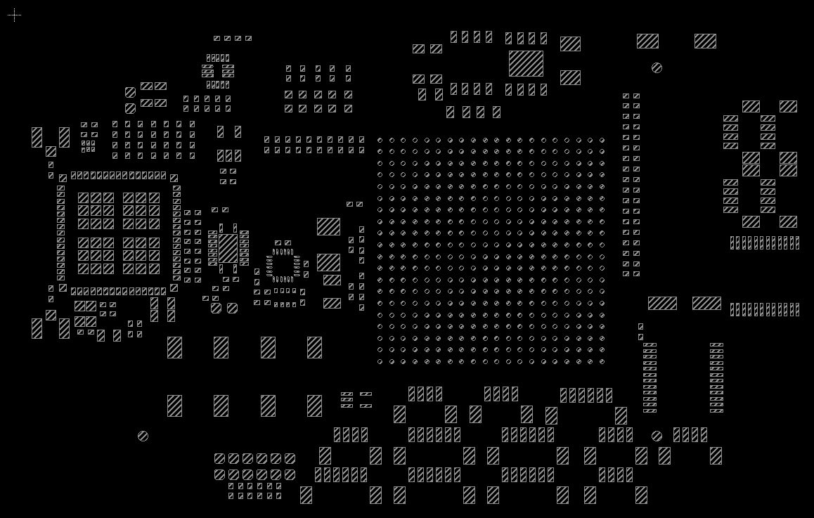
Layer 31-32: tCream/bCream
These layers contain all of the solder paste data for your surface mount components. You’ll usually find this layer being used by your manufacturer to make stencils for printing solder paste before assembling any parts.
When placing SMD packages, this cream information will automatically be generated for you. However, if you need to make an SMD footprint yourself, be sure to add the cream area smaller than the soldermask, so the two materials don’t overlap.
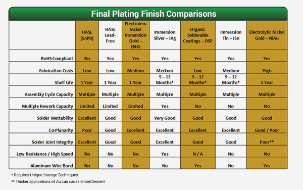
Layer 33-34: tFinish/bFinish
These two layers include data about any kind of special finish that your board requires, like plated gold or silver carbon. It can also include data about specific pads that need immersion gold plating.
Keep in mind, this layer will not automatically be generated, and you’ll need to draw it yourself if you need a special finish added to your board. However, if you’re just getting started with PCB design as a hobby you likely won’t use this layer as a special finish can be really expensive.
Layer 35-36: tGlue/bGlue
These two layers include both the top and bottom side of your glue mask. This mask is useful for securing components to your board that you expect to encounter stress during daily use, such as switches, jacks, or connectors.
Glue is typically applied by your manufacturer with one dot in the center of smaller components, and a few dots under larger parts like Integrated Circuits (ICs). Just like the Finish layers, you’ll need to draw this layer by hand if you need glue applied to specific areas on your board.
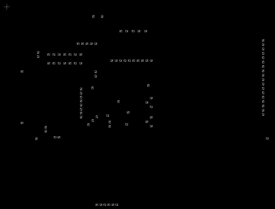
Layer 37-38: tTest/bTest
At the end of fabrication (creating your bare board) and assembly (stuffing parts on your bare board), your PCB will then be fully tested for any short circuits. This is where these two layers play their role by providing dedicated test points on both the top and bottom of your PCB for bare board testing or ICT (In-Circuit Test) equipment.
Autodesk EAGLE comes with some included test pads in its free libraries that you can use to quickly place on your board. Search for “test” in the Add dialog in EAGLE, then look for the testpad category. You’ll find a variety of test points you can add for through-hole and surface mount components.

Layer 39-40: tKeepout/bKeepout
Need to keep components away from specific areas on your board? These are the two layers you’ll want to use. By defining a keepout layer, your Design Rule Check (DRC) will be on the lookout for any components placed within your keepout boundaries and alert you with an error. You can also use the keepout area to define specific spacing requirements between components.
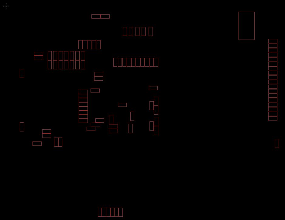
Layer 41-43: tRestrict/bRestrict/vRestrict
tRestrict and bRestrict are used to indicate where traces or copper should be removed on your board layout. By default, when you fill in a polygon with copper over a restrict layer, the restricted section will remove any copper.
This layer also comes in handy when using the autorouter in EAGLE, as it can prevent traces from being routed in defined areas. vRestrict will indicate where vias should not be placed, and this layer will also prevent the autorouter from placing vias in defined sections.
Layer 44: Drills
This layer contains all of the data for holes on your board that needs to conduct electricity, such as through-hole pads and vias. This layer can also be useful if you need to place a hole for a grounding bolt that will connect to your chassis.
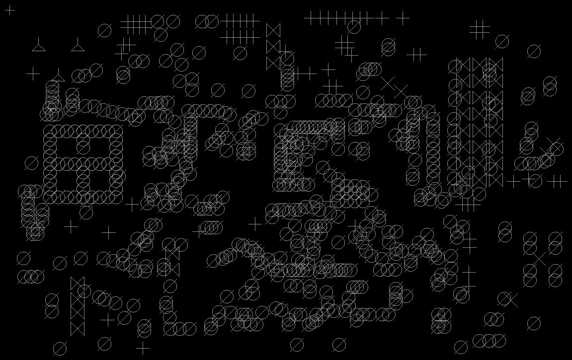
Layer 45: Holes
This layer is similar to Drills but contains all of the data for holes that don’t need to conduct electricity, like unplated mounting holes.
Layer 46: Milling
This layer is solely dedicated to the milling of holes, inner cutouts, and any other kind of contour that needs to be cut by your manufacturer. Keep in mind, this layer is not meant to define the dimensions of your board; you’ll need to keep that data on Layer 20. And unlike the Dimension layer, which can interact with your design rules, the Milling layer does not.
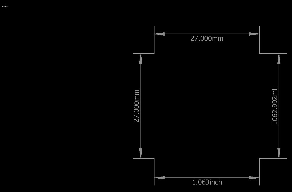
Layer 47: Measures
This layer contains all of the measurements you need to make on your board, like the dimensions of your board outline, or even the spacing between components. Keep in mind, this layer is meant for your own personal reference and will not be part of the data that gets sent to your manufacturer.
Layer 48: Document
This is the layer for all the supplementary documentation on your PCB. We recommend adding manufacturing notes on this layer for things like:
- Your PCB thickness
- Your layer stackup requirements
- Your soldermask and silkscreen colors
- Your desired copper type and weight
- Your impedance control specifications
- And your special finish requirements, if any
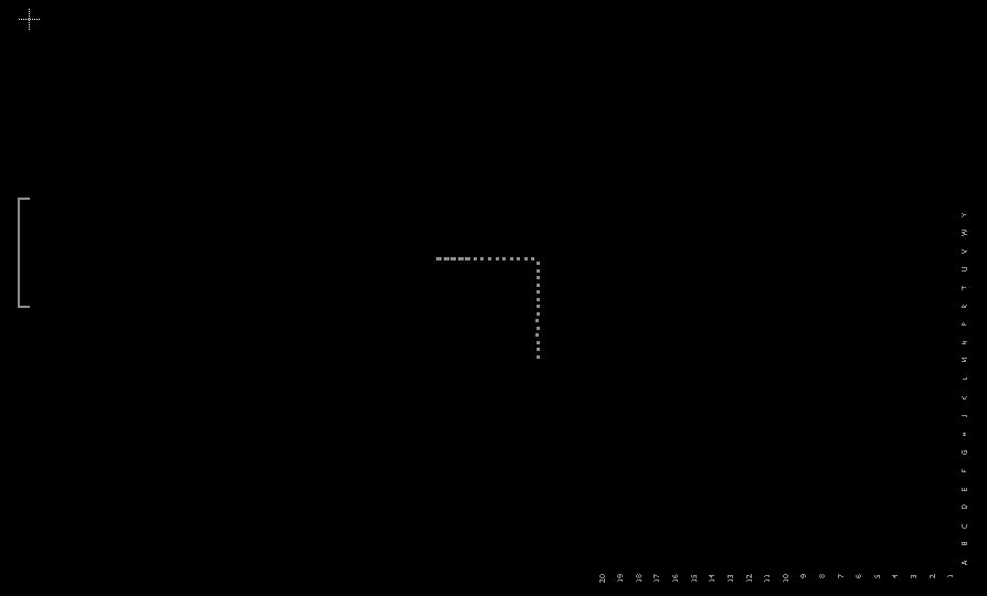
Layer 49-50: ReferenceLC/ReferenceLS
These two layers contain the reference marks for fiducials on your board. Never heard of these? They’re little marks placed on your PCB on the top and bottom layers that allow a pick and place machine to recognize where your board is located in physical space. At a bare minimum, we recommend including at least 2 reference marks on your design, but 3 is preferred by most manufacturers.
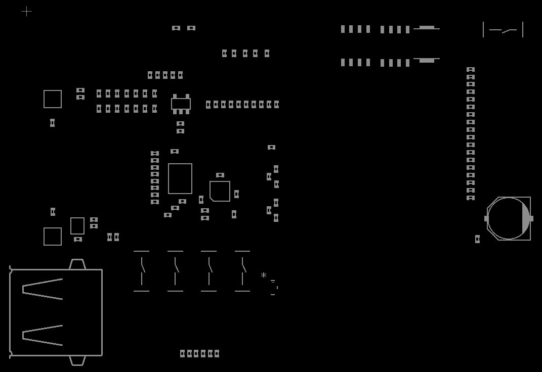
Layer 51-52: tDocu/bDocu
Last but not least we have the two documentation layers for the top and bottom of your PCB. These layers will not be included in your manufacturing files, but are instead a handy set of details to include when referencing or reviewing your design. Some things to consider putting on these layers includes both the mechanical dimensions of your components and enclosures.
Gotta Catch Em’ All
There you go, every single layer in Autodesk EAGLE, and what you need to know about them! Keeping track of all these layers might seem overwhelming at first, but as you dig into the intricacies of PCB design, you’ll see just how handy it can be to have this information available. Of course, we also can’t forget just how much of the data in your layers are going to be shipped off to manufacturing. We’re talking about things like the dimension of your board, copper pour areas, silkscreen, reference designators, and a whole lot more.
Need more signal layers than the free 2? Buy an EAGLE Premium Subscription today to unlock all 16 signal layers!
