& Construction

Integrated BIM tools, including Revit, AutoCAD, and Civil 3D
& Manufacturing

Professional CAD/CAM tools built on Inventor and AutoCAD
2 min read
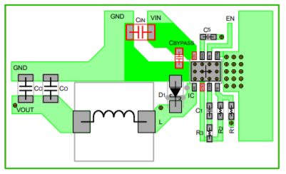
Buck Converters are an ideal solution for regulating a DC output voltage to be lower than a DC input voltage. These DC-to-DC converter circuits are much more power efficient than a linear regulator and are perfect when you need to convert mains into lower voltages. Today’s Everyday App Note from Rohm Semiconductor will walk you through a precise layout strategy to successfully design a buck converter circuit.

The layout process for a Buck Converter circuit is just as important as the rest of your circuit design. Poor converter layouts can often result in increased noise that affects your output switching signal, reduced efficiency of your regulator, and poor switching power supply stability.
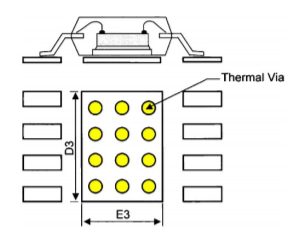
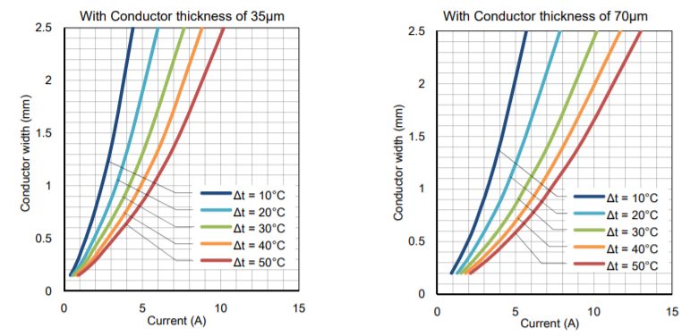
To ensure a successful layout process, Rohm has assembled a layout strategy that takes you from beginning to finish to design a Buck Converter circuit. These steps include:


Power supply reliability is no joke, and careful consideration needs to be made to the placement of each component and wire. This application note will walk you through all of the critical components to design a Buck Converter circuit from beginning to finish.
Download the PCB Layout Techniques of Buck Converter App Note now!
By clicking subscribe, I agree to receive the Fusion newsletter and acknowledge the Autodesk Privacy Statement.
Success!
May we collect and use your data?
Learn more about the Third Party Services we use and our Privacy Statement.May we collect and use your data to tailor your experience?
Explore the benefits of a customized experience by managing your privacy settings for this site or visit our Privacy Statement to learn more about your options.