& Construction

Integrated BIM tools, including Revit, AutoCAD, and Civil 3D
& Manufacturing

Professional CAD/CAM tools built on Inventor and AutoCAD
3 min read
This post is also available in: Deutsch (German)
Are you an electrical engineer looking for a cloud-based PCB design tool or an industrial designer looking to incorporate PCBs into your work? Fusion 360 Electronics is a comprehensive and affordable end-to-end solution that unifies MCAD and ECAD workflows like never before. In this article, we’ll explore five reasons why you should start using Fusion 360 Electronics. We’ll also highlight some common pain points with other solutions that Fusion 360 can help you avoid along the way. Let’s get right into it.
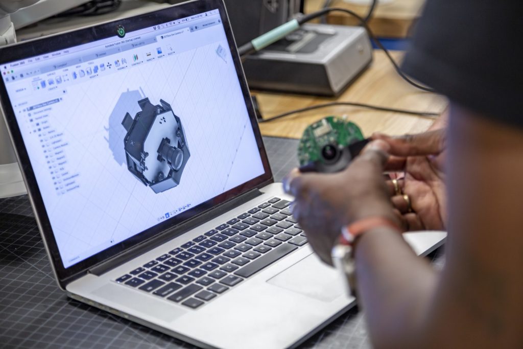
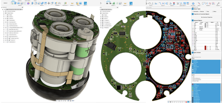
The primary value of Fusion 360 Electronics is its electromechanical capabilities. Fusion 360 Electronics allows mechanical engineers and electronic engineers to work in a single collaborative environment. Engineers can quickly adopt changes to a product’s design in a matter of moments because there’s no need for file conversions or translations. PCB design updates trigger an alert to the engineer to notify them of the changes. The engineer can then quickly and seamlessly adopt them.
In the same way, mechanical engineers can update changes to PCBs in the mechanical design workspace that the PCB designs will adopt. Engineers need this workflow for fine-tuning the placement of components that require external access. Additionally, all aspects of projects in Fusion 360 are versioned. Therefore, earlier iterations are easily accessible to review or re-adopt when needed.
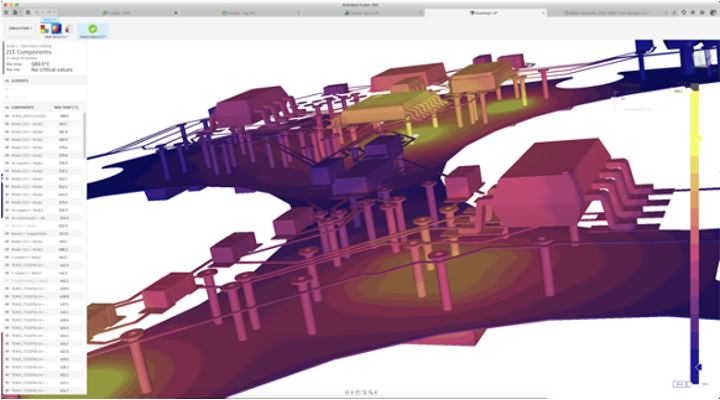
Fusion 360 offers an e-cooling solving workspace that PCB designers can utilize. This feature is possible because the 3D models of the PCBs consist of actual modeled and extruded bodies with identified materials.
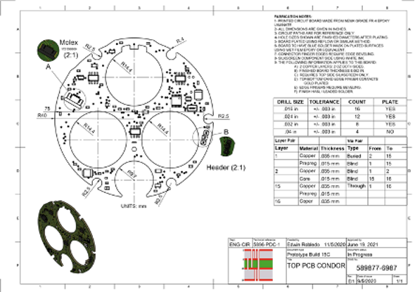
Fusion 360 also has a fabrication drawing workspace that works with 3D PCB models. No matter what product you’re hoping to produce, generating a fabrication drawing for your design is imperative. The fabrication drawing workspace in Fusion 360 helps designers and engineers avoid the hassle of exporting files to be used in a separate fabrication application. Additionally, Fusion 360 Electronics has implemented a design workspace environment that electronic engineers will genuinely value.
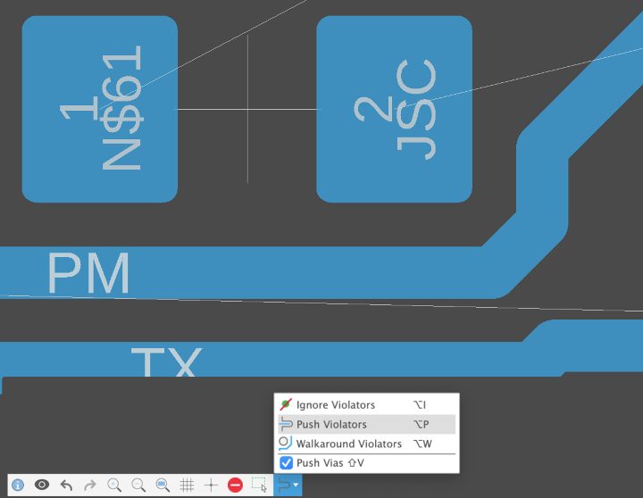
There are three types of routing environments in Fusion 360: fully manual, walkaround, and push and shove. The fully manual environment allows designers to move assets in the PCB workspace freely and alerts designers of manufacturing violations in real-time. The walkaround environment is an assisted interactive mode that helps engineers avoid manufacturing violations by forbidding them to place assets in violation areas. Finally, the push and shove environment is a term usually used solely for routing traces. In Fusion 360 Electronics, however, we took push and shove to the next level. While moving parts, traces, and other assets on the PCB, Fusion 360 will push the other assets out of the way to accommodate the part being move and avoid manufacturing violations.
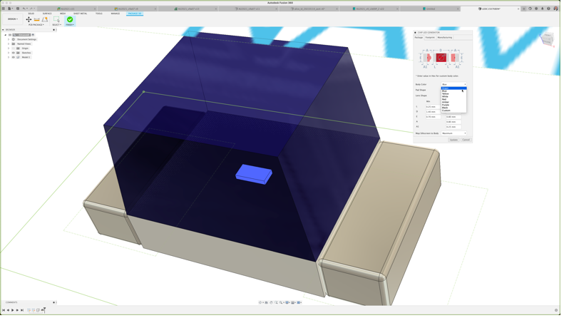
The foundation of all electronic designs is part libraries. Even if you constantly add parts to your parts repository, it’s tough to have them all. Therefore, there are occasions where engineers need to build their components. All PCB designers dread making custom components, but switching to Fusion 360 enables them to avoid this task. Thanks to the package calculator in Fusion 360, engineers can simply select their desired component template to enter the mechanical details of the required chip. In a matter of moments, they will have the component’s footprint and 3D model at their fingertips.
You can visualize the PCB within the enclosure by providing a 3D model environment of your electronic design. You can invoke interference checks in the design workplace, and these checks will show you errors from the selected bodies. With the “Edit in Place” capabilities in Fusion 360, you can change your component’s location. These modifications will automatically cascade across the design environment, and the PCB will adopt them. With the part location corrected and adopted, now you can make the necessary changes to the PCB. The broken process of converting and exporting files is error-prone and time-consuming. With Fusion 360 you will be notified of errors and also be able to see them.

There you have it — that’s five compelling reasons why you should switch to Fusion 360 Electronics if you haven’t already. Want to learn more about how Fusion 360 Electronics can enhance your team’s PCB design and manufacturing processes? Visit the links below.


By clicking subscribe, I agree to receive the Fusion newsletter and acknowledge the Autodesk Privacy Statement.
Success!
May we collect and use your data?
Learn more about the Third Party Services we use and our Privacy Statement.May we collect and use your data to tailor your experience?
Explore the benefits of a customized experience by managing your privacy settings for this site or visit our Privacy Statement to learn more about your options.