& Construction

Integrated BIM tools, including Revit, AutoCAD, and Civil 3D
& Manufacturing

Professional CAD/CAM tools built on Inventor and AutoCAD
5 min read
PCBs rely on layers of copper that are etched away to create tracks (sometimes called routes). These tracks connect components on the PCB to form circuits. In this blog post, we’ll examine the things to watch out for when using multiple layers of copper in your PCB layer stack.
The simplest PCB consists of only one layer of copper and is used for inexpensive PCBs with few components.
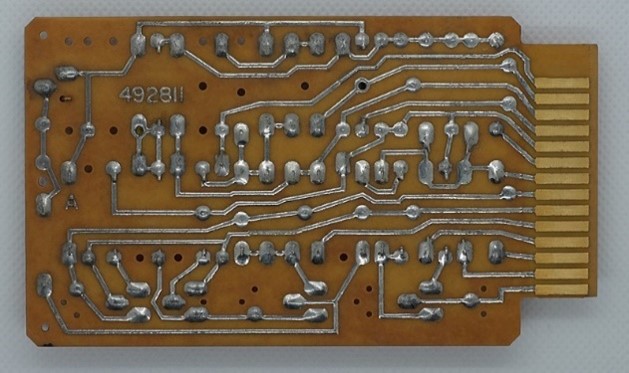
Double-sided boards are prevalent for moderately complex low-component count PCBs. They are inexpensive as the PCBs are pre-manufactured with copper foil glued on both sides. Most PCBs today need more layers to route component connections as required.
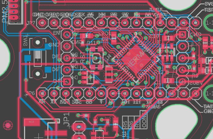
Power planes are solid planes of copper sandwiched into a PCB. There comes a time when two layers aren’t enough, and even more layers are necessary. Sometimes extra layers are used to provide power planes. This provides excellent power supply decoupling acting like a huge power supply decoupling capacitor that is good for frequencies much higher than conventional decoupling capacitors.
But they also provide another crucial function: a path that constrains the electric field to a small area, minimizing cross-talk and EMI (Electro-magnetic Interference).
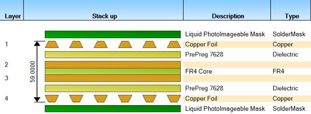
The layer stack is simply the order and spacing between the layers of your PCB. The simplest and least expensive way to manufacture a four-layer PCB is to attach two copper foil layers to the top and bottom of a double-sided PCB. The top and bottom layers are separated by fiberglass cloth pre-impregnated with epoxy that has not cured. This pre-preg, often called, is soft and pliable and will form itself around existing traces etched out of the middle double-sided PCB (called the core).
When introducing electric circuits, we teach that voltage “pushes” electron current through conductors. This is not the case. It’s the electric field that applies the force. Your stack-up needs to consider the electric field and keep it from spreading to places where it can interfere with signals and power rails.
The order of layers in the stack-up is critical in enabling a PCB designer to contain the field and prevent cross-talk or common mode currents from injecting noise into signals or power rails.
Autodesk Fusion 360 comes with a layer stack manager that allows you to define and visualize your layer stack.
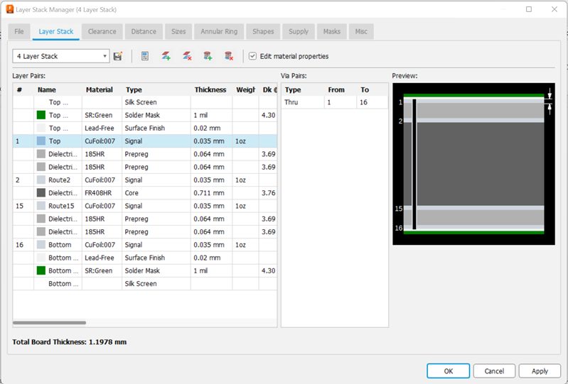
In Fusion 360, layers have numbers from 1 to 16; however, when discussing layer stacks, we often refer to them by their order on the PCB. In this four-layer example, layer 15 and 16 are layers 3 and 4.
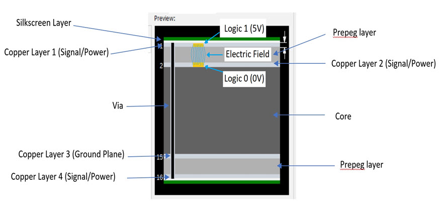
It’s essential to organize your layers to contain the electric fields and minimize them interacting with each other. Consider this poor four-layer stack-up with a signal/power plane on layers 1 and 2, a ground plane on layer three, and signal/power on layer 4.
It has three layers for routing, but why is this a poor stack-up? To answer that question, we need to think about how electric fields will establish themselves on the board. Consider two traces, one on layer one and one on layer 2. Suppose we are using these traces for digital signals. Suppose the layer 1 trace has a logic 1 or 5V present on it and layer 2 a logic 0 or 0V. This will establish an electric field between the two traces.
The problem is that signals from layer one will also create an electric field from layer 1 to layer three the ground plane.
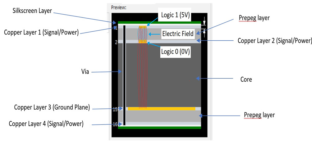
The 5V signal on layer one will also develop a field (shown in red) between layer one and the ground layer (layer 3). The layer one and layer two fields (shown in blue) will couple onto the ground because they overlap the Layer 1 and layer 3 fields. This makes the ground plane noisy as well.
Fields interfering with each other causes SI (Signal Integrity) and PI (Power Integrity issues). It’s worth noting that the signals from layer four couple to the ground plane on layer 3 are well contained and do not interfere with each other.
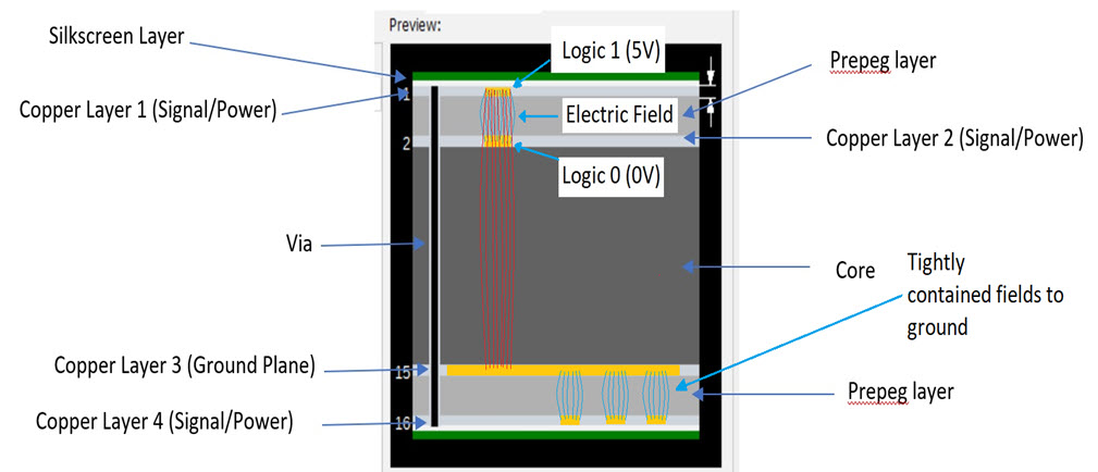
And that’s a hint as to how the stack-up can arrange to minimize these interactions.
With this stack-up arrangement, the electric fields associated with signal layer two will be tightly coupled to the ground layer one ground plane.
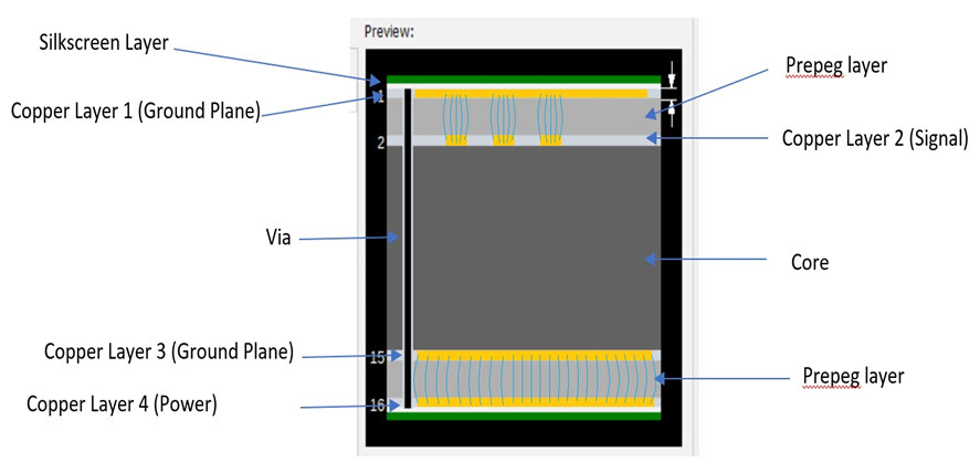
Of course, this better stack-up has one major problem: it has only one layer for routing signals.
Ideally, we would just add more layers to our PCB. For example, here is a good six-layer stack-up. But again, not very cost-effective as there are only two routing layers.
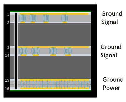
We need to add a signal layer and combine it with power pours. Here’s a six-layer stack that does just that.
The fields are tightly contained by the ground planes beneath them. Large power plane pours also increase supply and ground capacitance, improving PI (Power Integrity).
A 4-layer stack with signal and power on layers 1 and 4 and ground in the middle on layers 2 and 3 also works well to keep fields contained. Or better still, sig/pwr and sig/pwr and as shown in b) as it allows for stripline between the two grounds on layers 2 and 4.
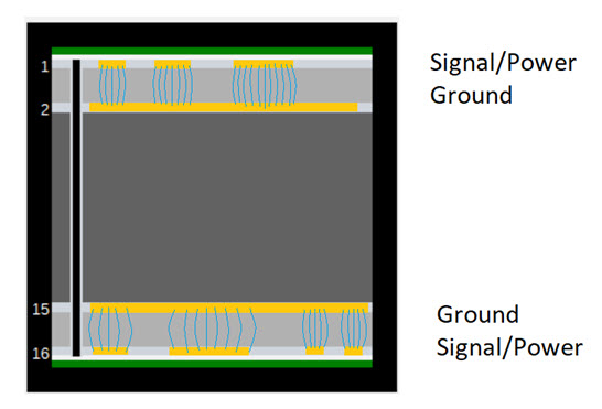
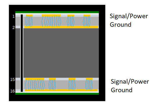
Notice how all these layouts minimize the interactions between signal and power fields by making sure the fields do not overlap.
Again, let’s look at a bad layout stack where fields overlap.
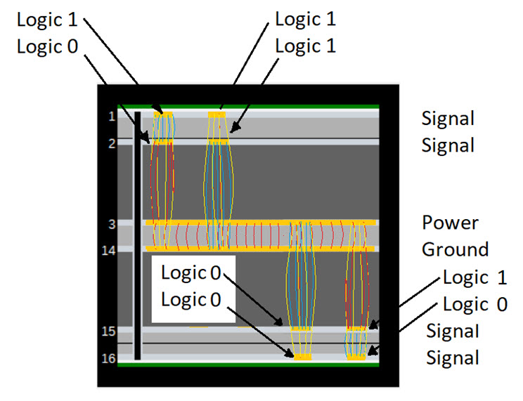
Getting the stack-up right is the first step in producing a PCB that minimizes SI and PI issues. Electric fields from signals and power are present between layers of copper and cause current to flow. It is crucial to ensure that electric fields are contained and do not overlap. Poor stack-ups result in overlapping fields and result in SI, PI, and EMI problems. Good stack-ups tightly constrain electric fields and minimize SI, PI, and EMI issues. Make sure you get your stack-up right. In part 2, we examine how to route between layers in ways that reduce the spread of electric fields.
Ready to work on your next design in Fusion 360? Get a 30-day free trial today.

By clicking subscribe, I agree to receive the Fusion newsletter and acknowledge the Autodesk Privacy Statement.
Success!
May we collect and use your data?
Learn more about the Third Party Services we use and our Privacy Statement.May we collect and use your data to tailor your experience?
Explore the benefits of a customized experience by managing your privacy settings for this site or visit our Privacy Statement to learn more about your options.