Is there anything you should be aware of when routing between multiple PCB layer stacks? Let’s explore in this blog post.
PCBs with multiple layers exist because it’s impossible to route today’s complex circuits on only one layer. This means eventually, the trace you’re routing will have to continue on another layer. Let’s explore everything you should be aware of when routing between multiple PCB layer stacks.
Routing Between PCB Layer Stacks
Yes, there are important things to consider when routing between layers. We must ensure that the electric field associated with the signal does not spread into the dielectric sandwiched between. You may recall from part 1 (Fundamentals of PCB Layer Stacks – Part 1) that the electric field moves current through traces and that it is essential to structure our layer stack to minimize the overlap of electric fields. Here’s what we don’t want, as fields from the signal layers overlap with power fields:

A better stack-up has ground planes adjacent to signal/power plane layers, as shown below:
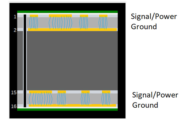
When moving from one signal layer to another, we should always ensure the signal layer we move to is on the other side of our ground return. This way, the field associated with the signal will be tightly coupled and will not spread out:
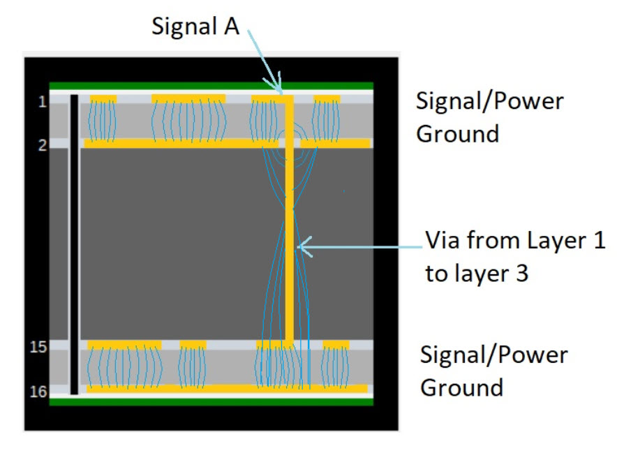
layer 1 to layer 3
Let’s contrast that with a trace that travels between layers on a poor stack-up:
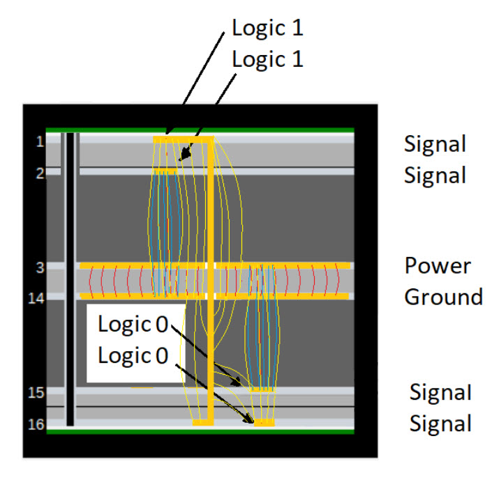
Here we see that the electric fields spread out and interfere with other fields. This will cause SI and PI, and EMI issues. These examples also highlight the importance of the ground plane being close to the signal trace. Consider the example below where the ground isn’t close to the signal trace:
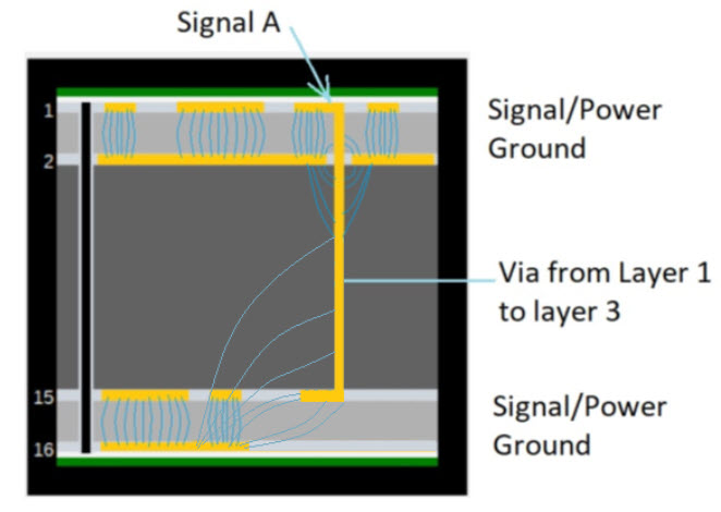
Once again, the electric field is spreading out and overlapping other fields. Always try to place ground underneath your signals.
Often PCB designers will place a ground directly beside the signal via to ensure that the field is tightly contained:
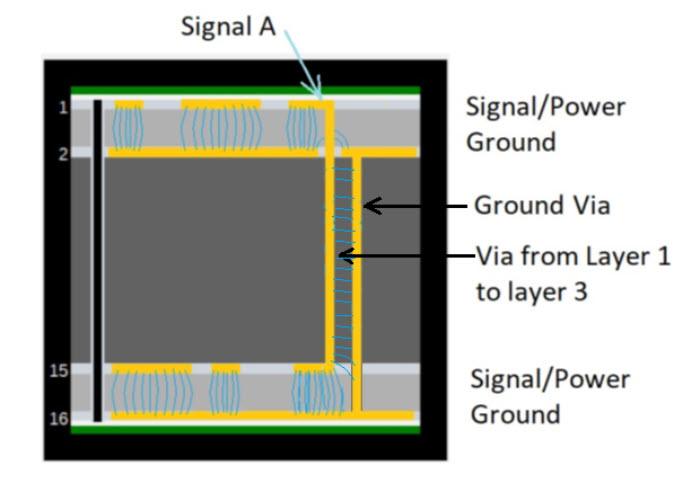
Routing signals from one layer to another can result in SI, PI, and EMI issues due to overlapping electric fields. To minimize the overlapping of fields, ensure ground planes are underneath the signals, route from one side of a plane to the other, and use adjacent ground vias when possible. This will go a long way to minimizing SI, PI, and EMI issues.
Check out Part 1 of this series to learn what to watch out for when using multiple layers of copper in your PCB layer stack.
Ready to create your first design in Fusion 360? Start with a 30-day free trial today.
