& Construction

Integrated BIM tools, including Revit, AutoCAD, and Civil 3D
& Manufacturing

Professional CAD/CAM tools built on Inventor and AutoCAD
12 min read
USB connectors are everywhere these days. Learn the best practices for routing your PCB traces to your USB 2.0 connectors.

You’re most likely familiar with USB connectors since nearly all electronic devices use them for charging, powering up, or data transfer. Since streaming data has become commonplace, it’s necessary to implement techniques to speed up USB connectors’ data transfer speeds reliably. This blog will teach you the best practices for routing your PCB traces to your USB 2.0 connectors.
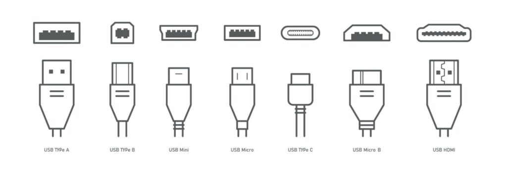
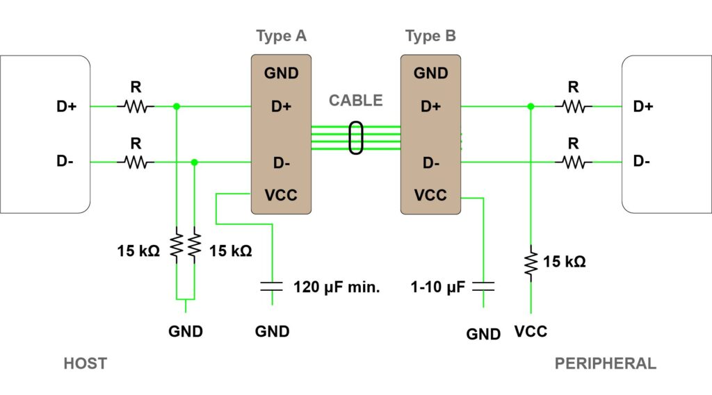
Before we begin providing details on routing, I’d like to give you an overview of USB pinouts. As mentioned earlier, USB devices are for data transfer. They are also for battery-charging electronic devices: mobile phones, players, laptops, tablets, and other gadgets.
Creating a high-quality USB connection requires knowledge of USB Standards, the ability to read diagrams, and guidance on the type of connections. Knowing the wires’ classification, colors, and purpose is necessary. Trouble-free long cable operation is ensured by correct wiring. USB 2.0 connector pins type A and B
This cable is commonly found connecting computers to printers and scanners. The colors of the wires found in this cable are:
These cables have smaller connectors and connect to cell phones and other devices that do not have the space for larger USB connectors. The colors found on these connectors are:
Most cables have a Shield cable; it has no insulation and is used as a shield. It is not labeled and is not assigned a number. A universal bus has two types of connectors. They are marked with an M for (male) and F (female).
Version 3.0 of the bus has a ten or 9-wire connection. Pin 9 is used for the Shield wire, which is missing. Pin assignment is such that it allows for older devices to be connected.
The plug;
USB 2.0 is also a high-speed USB. In April 2000, it was released and is supported by nearly all USB-compatible devices.
USB 2.0 devices have a maximum data transfer rate of 480Mbps, higher than USB 1.1.
The USB 2.0 standard supports the Mini-A, Mini-B, and Mini-AB connectors.
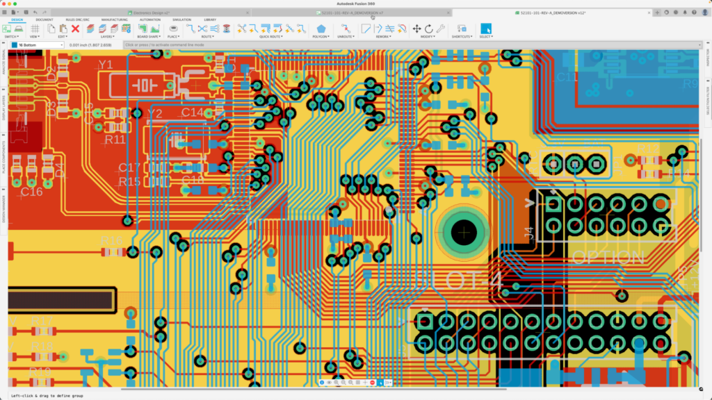
Many believe that routing PCB traces on a PCB design is easy. Routing a board for low-speed signals is considered a relatively straightforward process, but this couldn’t be further from the truth for high-speed USB signals.
In the past, when low-speed TTL DIP components were used on simple boards, that might have been accurate. Today’s designs are much more complex and need to meet specific routing criteria for the component to be operational. A PCB’s traces may require detailed design specifications to be met while routing o ensure signal integrity. Although traces might have routing specifications, you can set up and meet the design criteria for your traces with today’s more advanced PCB routing techniques and capabilities.
The routing methods you’ll use for your board depend entirely on your routing topology and signaling standard.
Don’t worry if you’re designing a PCB for the first time and are about to begin the routing stage; we’ll show you how to do it and tell you which routing specifications your PCB needs to meet.
Starting PCB Routing
All PCBs must have copper traces, which connect components on the surface or interior layers. The routing technique used in your PCB will rely on several criteria.
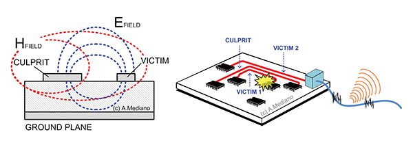
Your goal as a designer is to balance all these factors and choose the ones that are most important for specific connections. Although high-current DC designs require significant traces that don’t necessarily have particular impedance, you might have to route signals away from the high-current paths to minimize noise., High-speed designs depend on controlled impedance with differential pair routing rules.
Let’s look at some of the simpler boards’ routing requirements to start before moving on to more complex designs.
If your design is not working at high speeds, it will not have width requirements to avoid crosstalk issues. You are generally free to choose a trace width that easily supports your component pins and leads if your traces only need minimal current.
These designs use trace widths between 5 and 15 mils since they are small enough to route directly into component pads. The diagram below shows a simple op-amp example with traces running between a low-speed IC, some resistors, and capacitors.
These simpler designs typically don’t have to worry about impedance, common routing topologies, or excessive currents.
Today’s boards may require impedance-controlled trace design and routing principles to assure signal integrity, even if they only have primary MCU and low-power stages. To ensure dependability and signal integrity, designers must define the trace requirements for their connections.
Your signaling standards will determine your routing needs, including total maximum length, impedance standards, and the permitted length mismatch in differential pairs or parallel buses.
You can create design rules and classes for individual nets in your design once you’ve determined any routing requirements in your board. As you route traces, your routing tools will use these requirements to determine the trace width, which requires defining minimum or maximum trace widths in your design rules.
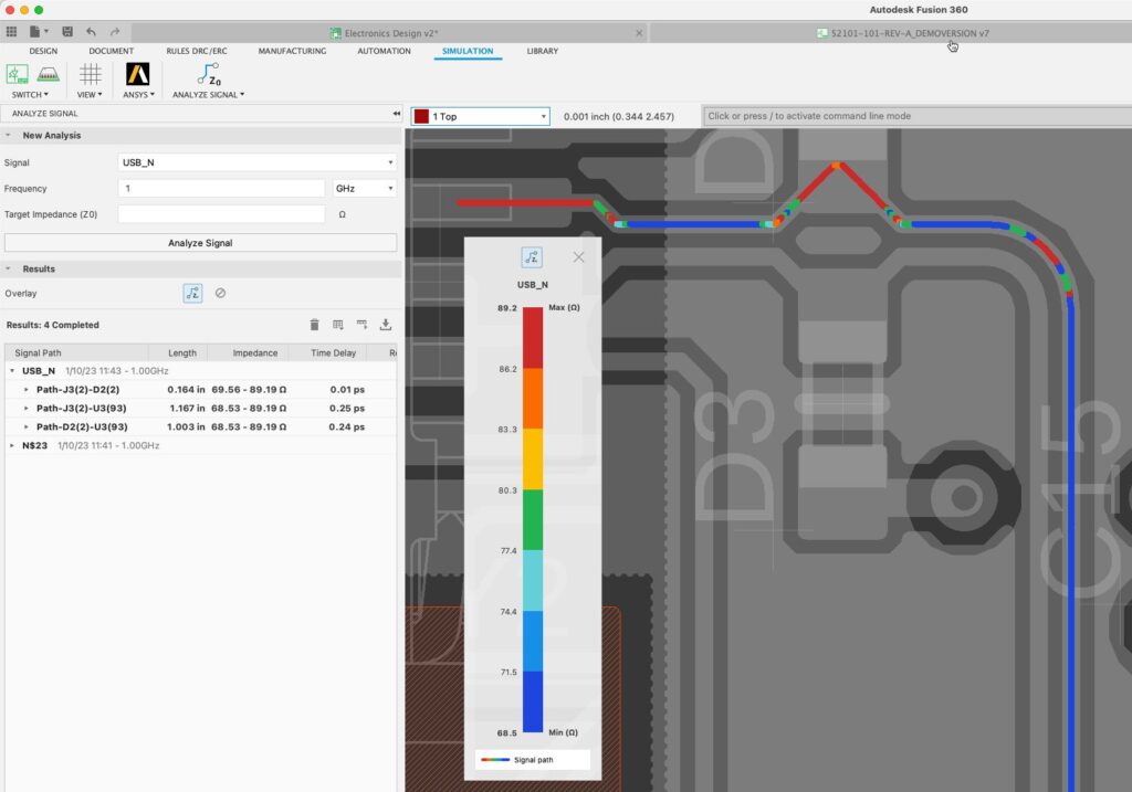
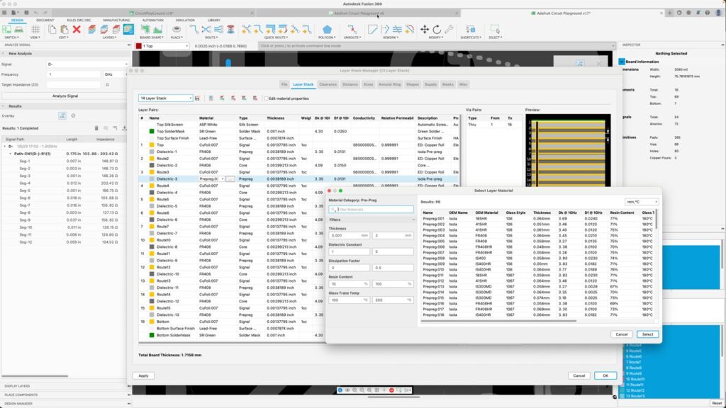
You must choose from several approaches to determine the impedance when you need to regulate it in your PCB layout. You can use formulas to determine the impedance in your design, or you can use an app specifically designed for this purpose. With the Fusion 360 Signal Integrity Extension, powered by Ansys, you can review the selected signal impedance of your lines and get insights on the target impedance.
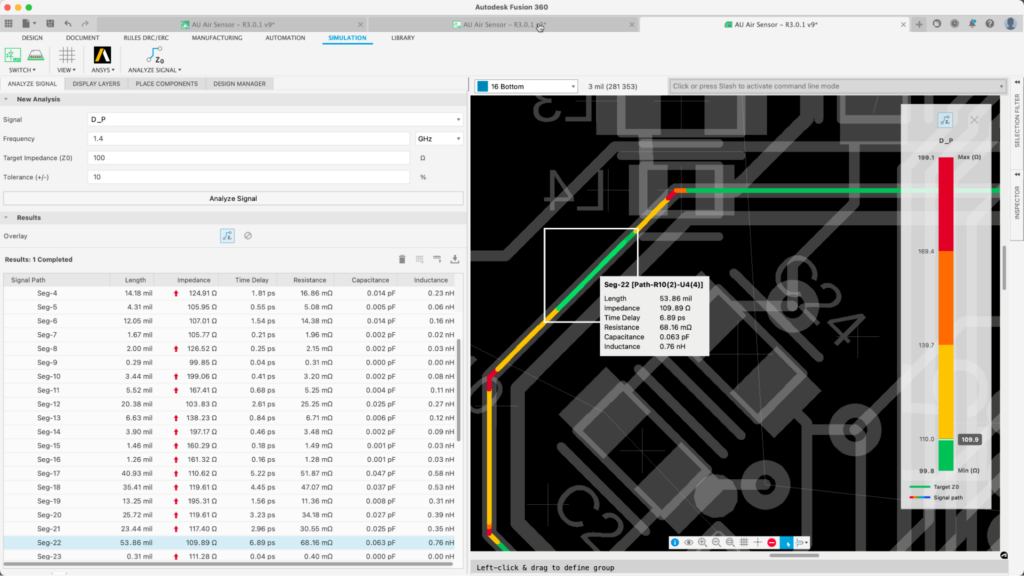
In PCB design software with a built-in impedance calculator function, you can calculate impedance quickly. This kind of functionality is present in only some PCB design programs, and those with it have varying degrees of accuracy in their output. The best PCB design software will have an electromagnetic field solver that automatically analyzes the trace geometry, which is currently in the Fusion 360 Signal Integrity Extension.
These tools will show how trace width and pair spacing changes affect target impedance and use the copper height and dielectric values to influence impedance results.
Trace routing topologies specify how traces carry to and from component inputs and outputs and how they branch off one another to reach different components.
In DDR routing, for instance, a single bus branch-off is used to reach numerous design components using a fly-by topology.
SPI uses a comparable bus design, but termination is implemented at the bus’s load points. When a design calls for a single component to communicate with multiple loads through a single IO interface, other components may use point-to-point topology to get to multiple components.
Ensure you are familiar with the routing topology required by your signaling standards and whether impedance control is necessary for those traces.
PCB layout for high data rate transmission is quite challenging, especially given the care with which the traces must be laid. There are a few guidelines that you should use to get the layout right for any high-speed PCB layout:
The design and routing of PCB stack-ups closely algin to signal integrity.
Signal integrity is mainly determined by how your plane/GND/PWR layers are arranged The easiest method to ensure your design will maintain signal integrity and minimize EMI is to place a ground plane adjacent to signal layers.
These recommendations, plus the above routing rules, should help prevent or reduce many signal integrity issues and guarantee your board will work.
Interactive routing tools are the most cutting-edge solutions that can assist you in following fundamental PCB routing rules.
In other words, using these semi-automated tools, you can specify routes for a collection of signals. The routing tools will place the traces so that they automatically follow your design guidelines.
Establishing design rules for your nets and classes of nets ensures that they automatically adhere when routing.
Advanced PCB design programs can help you stay productive as you work to complete your PCB layout and route traces around your board. Many freeware and open-source design programmers force you to do everything manually.

You can route traces in your PCB layout by pointing and clicking on different parts of the board. Your intended DRC (Design Rule Check) assigns the trace width that will be used along the route of the selected signal, eventually extending across the layout to the needed location.
As you route traces in your layout, routing tools in your PCB editor application can automatically turn corners (often at a 45° angle). As you move traces between components on the PCB, they can insert vias.
Prepare a plan for several routes before you begin routing PCB traces to make sure you use vias sparingly or need to add extra layers to complete the board.
Your PCB routing technique will depend on your PCB layout; if the PCB layout has fewer crossing nets, routing traces with fewer layer transitions would be more challenging.
Sometimes it’s necessary to begin with the most straightforward routes first because they’ll show you which ones require the most time and work to complete routing in the PCB layout.
To design and route a high-speed printed circuit board, you need to follow certain design rules for optimum performance. In the following, we will consider these trends and issues:
Complete the routing of a PCB design can be one of the most demanding PCB-related tasks. This becomes more difficult if the board size is small and the various components are hard to find. This guide provides essential guidelines, tips, and rules to help you easily design your high-speed PCB using USB 2.0 connectors.
Ready to expand your Fusion 360 PCB capabilities? Start with a free trial of the Fusion 360 Signal Integrity Extension today.

By clicking subscribe, I agree to receive the Fusion newsletter and acknowledge the Autodesk Privacy Statement.
Success!
May we collect and use your data?
Learn more about the Third Party Services we use and our Privacy Statement.May we collect and use your data to tailor your experience?
Explore the benefits of a customized experience by managing your privacy settings for this site or visit our Privacy Statement to learn more about your options.