& Construction

Integrated BIM tools, including Revit, AutoCAD, and Civil 3D
& Manufacturing

Professional CAD/CAM tools built on Inventor and AutoCAD
5 min read
This comprehensive guide explores PCB design and the careful approach needed for PCB layout to ensure smooth transitions from blueprint to tangible product, focusing on both Design For Assembly (DFA) and Design For Fabrication (DFab) perspectives.
In the realm of electronics, the design and production of PCBs are alike to the construction of a city’s infrastructure. Just as urban planning requires a keen eye on the layout for utilities, roads, and buildings, PCB design demands a meticulous approach to ensure a seamless transition from blueprint to tangible product. This extensive guide delves into PCB circuit board design from the Design For Assembly (DFA) and Design For Fabrication (DFab) perspective.
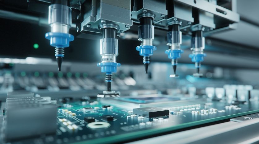
Before we begin our optimization journey, let’s decipher the PCB assembly process. Production commences after design approval, whether it’s a flexible PCB or an HDI, transforming the design into a tangible form. However, the ‘bare board’ is merely a skeleton awaiting the sinews and organs—the electronic components that give it life and function.
Often, particularly among individuals who have yet to become experts in printed circuit boards (PCBs), the issue is that the board’s initial design fails to consider the assembly process. Instead of considering the larger context of how the board will function within the product or application, they solely focus on its design.
Another essential aspect to consider is the availability of components. For the process of assembling circuit boards to run smoothly and for the overall production to be effective, the assembly vendor must have the necessary components on hand when the boards are received. These components must be readily available for the entire process to be completed on time, diminishing the benefits of a fast-turnaround approach to board production.
DFA urges designers to consider the assembly stage right from the inception of the PCB design. Component placement is vital; too intimate a placement could spell disaster, leading to malfunction or compromised performance. Here’s how to avoid these pitfalls:
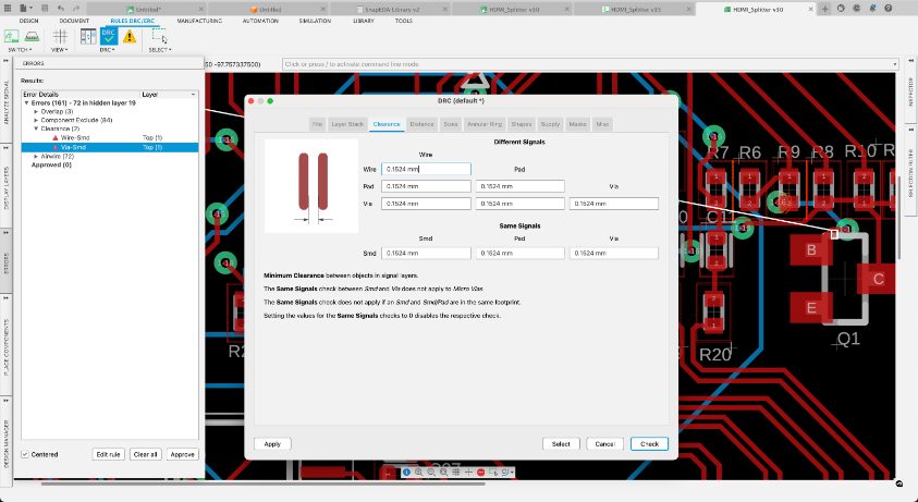
Imagine the components on your PCB as pieces on a chessboard. Each piece must have adequate space for comfort and strategic movement. Similarly, components need room for easy placement, soldering, and potential rework. Incorporating sufficient space prevents shorts and allows for better heat dissipation, which is crucial for the reliability of the PCB.
The primary issue in assembly is the need for pin 1 indicators or polarity/orientation indicators on the silkscreen, which hinders the process. Approximately 75% of the orders received by a facility need proper identification of the pin 1 location for ICs, or they need to accurately represent the polarity of certain components, such as capacitors, diodes, or LEDs.
Setting up component regulations, requirements, and proximity rules in your design software is essential to avoid potential problems. Board experts have specific guidelines for the spacing between different types of components. For instance, discrete components such as capacitors and resistors should always be spaced at least 10 mils apart, with a preferred spacing of 30 mils. This precautionary measure can prevent proximity-related issues that cause delays or complications during assembly.
While machines populate most PCBs with components, humans also interact with them. Designing with both in mind ensures a machine-efficient and human-friendly process. Features like breakout tabs and hand-soldering areas can make a significant difference.
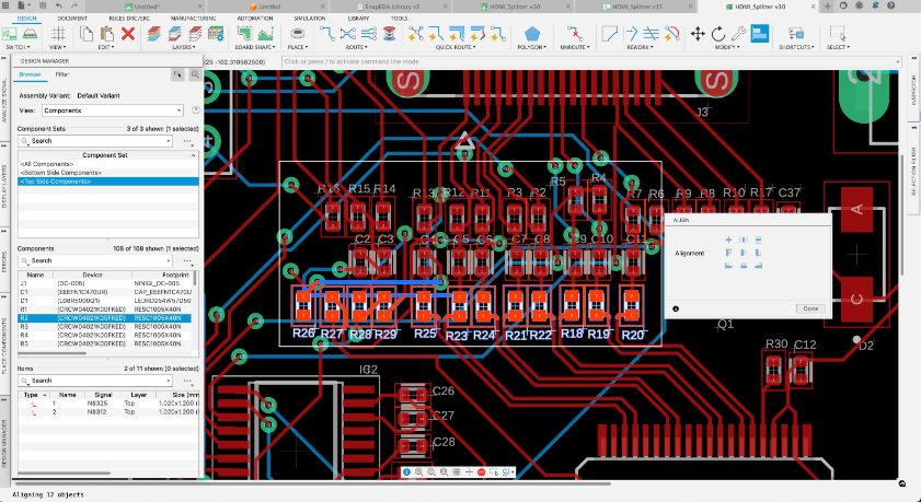
Complexity is only sometimes a virtue in PCB design. A more straightforward design can often lead to fewer errors during assembly. Minimizing the variety of components reduces the complexity and time involved in assembly.
TIP:
Combining different technologies on a PCB, like mixing through-hole and surface mount, is generally not recommended due to increased complexity and cost. It’s more efficient to use uniform technology across the board. Placing all such components on one side simplifies manufacturing when using a through-hole. Early in the design process, electrical engineers and PCB designers must select the proper component package sizes, weighing the ease of assembly against the necessity of smaller sizes. Significant components are often preferred if they meet design requirements, ease assembly, and increase yield.
Additionally, considering lead times for components is critical; parts with longer lead times should be identified early and ordered in advance to ensure they’re available when needed, potentially delegating this task to the assembly vendor to streamline the process.
DFab, on the other hand, is all about ensuring the board can be manufactured without complications. This involves:
Choosing suitable base materials can prevent issues such as warping or delamination. Different materials will behave differently under the stresses of assembly and in their operational environment.
It is important to avoid mixing lead-free components with those not designated for lead-free assembly. In cases where a component must be assembled using lead-free methods and traditional lead-based solder is not suitable, the entire board must be assembled using lead-free techniques, and all components must be compatible with lead-free assembly.
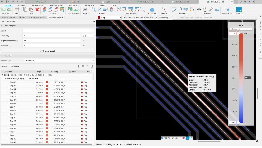
When designing a printed circuit board (PCB), the arrangement of layers—the stackup—alongside careful impedance planning plays a critical role in determining the board’s performance. Understanding the electrical requirements of your design and meticulously planning the stackup will considerably impact the signal integrity and the efficacy of power distribution. By doing so, designers can minimize issues like signal loss and electromagnetic interference, which are crucial for the reliable operation of high-speed circuits. Additionally, proper impedance planning ensures that the PCB will meet the necessary electrical standards and function correctly with other components in a system, thus optimizing the final product’s overall performance.
Beyond design intricacies, the availability of components is paramount. The absence of necessary components upon board receipt can delay the entire process, undermining the rapid production of PCBs.
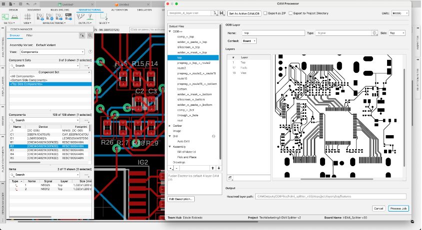
Mastering PCB design is about balancing the interplay of DFA and DFab. It’s about envisioning the end product, acknowledging the capabilities and limitations of assembly and fabrication, and integrating these elements into the design process.
Focusing on DFA and DFab allows designers to optimize their board designs on the first attempt, ensuring a seamless and efficient production process that yields high-quality, functional PCBs.
By clicking subscribe, I agree to receive the Fusion newsletter and acknowledge the Autodesk Privacy Statement.
Success!
May we collect and use your data?
Learn more about the Third Party Services we use and our Privacy Statement.May we collect and use your data to tailor your experience?
Explore the benefits of a customized experience by managing your privacy settings for this site or visit our Privacy Statement to learn more about your options.