& Construction

Integrated BIM tools, including Revit, AutoCAD, and Civil 3D
& Manufacturing

Professional CAD/CAM tools built on Inventor and AutoCAD
9 min read
One of the most challenging aspects of PCB design is addressing the total wealth of technical and manufacturing constraints. This blog explores why our design rules system is the perfect partner for this.

Before you start placing parts on the PCB and routing, it is a good idea to understand the design constraints your PCB should follow to work correctly and be manufacturable. The more constraints you’re empowered with before you start working on the PCB, the more issues you’ll be able to avoid.
Fusion Electronics has adopted a flexible design constraint system to satisfy the most complex design and manufacturing criteria. For your convenience, we have split this into two levels of constraints. Design Preference will now be dedicated to global PCB settings such as Layer Stack, Layer Material Properties, Annular Ring, Supply, and Mask properties. These are parameters that will apply to the entire design. Design Rules will be split between General Rules and Custom Rules.
“Defining PCB design rules early during the design stage is essential to ensure performance and manufacturability requirements are met from the outset. By establishing constraints early on (such as trace widths, spacing, layer stack-up, and minimum dimension requirements), designers can avoid costly rework due to signal integrity issues or fabrication process compliance before these issues ever arise. Early rule definition also streamlines the design workflow, reducing costly iteration cycles and ensures that the final product adheres to industry standards. It minimizes the risk of errors that could compromise functionality or delay production.”
– Melisa Kaner, MEng
Product Manager Autodesk Fusion Electronics
An excellent example of the need to override global settings is for Power Rails on the PCB. Power rails usually require a wider trace width value that is more significant than your analog and digital traces. This is where Net Class empowers you to create exceptions to the global preferences. Net Class and DRC work great, but the complexity of the latest design requirements requires more sophisticated constraint control.
 Thursday, March 13, 2025 |
  10 am PST | 1 pm EST | 6 pm GMT
Before diving into the details, here are a few key points to highlight:
The General Rules define the bare minimums of the manufacturing process. Notice that each parameter has an Enable option in the second column. This lets you turn off an unnecessary rule you plan to overwrite with custom rules.
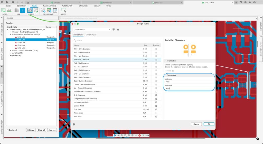
The values can be easily changed by simply typing the value that will satisfy your design constraints. Please note that the parameters are divided into minimum and preferred. The minimum will be the smallest value acceptable for your design, while preferred is the value you want to use whenever possible. The preferred value can never be smaller than the minimum. The top right of the dialog provides graphics of what this constraint refers to. If you are an EAGLE user, you will be familiar with these settings; the only difference is the improved interface.
“Having a minimum and a preferred setting in PCB design rules provides flexibility and helps balance performance with manufacturability. The minimum setting defines the smallest or tightest constraint the design can tolerate. However, working strictly to these limits can increase cost and complexity in manufacturing. Preferred settings, however, represent design conditions that are easier to produce, more reliable, and often less expensive. By defining both, designers can optimize for performance while allowing room for cost-effective and dependable manufacturing practices, improving yield and reducing the chance of defects.”
– Jorge Garcia, BSEE
Sr. Community Manager Autodesk Fusion
PCB Constraints customization and flexibility are paramount for successful design; this is where the Custom Rules implementation truly shines in Fusion Electronics. Custom Rules are tailored to specific design requirements. For example, a high-frequency PCB might have different trace widths than what’s defined in the general rules. In these cases, you can override the global settings with custom rules for specific nets or components. These customizations allow for more flexibility in unique or complex designs that might not fit within the general manufacturing limits.
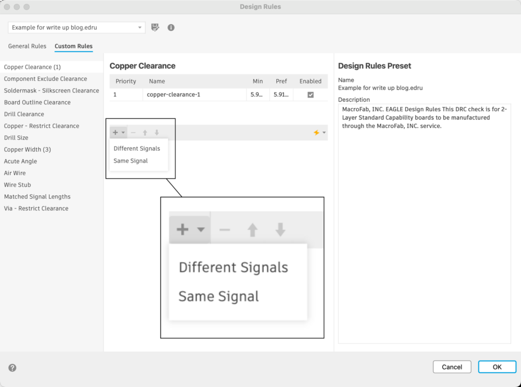
The Custom Rules tab will have a list of options. You are not limited to these options; you can add more as necessary. In the copper clearance example, the first step involves selecting whether the defined clearance applies to the same or different signals. Each rule added will automatically be assigned a priority. This is the order in which the PCB will be checked. The rule’s priority (order) is also used when getting the best applicable rule for interactive route, differential-pair routing, multi-route, and copper pour. Also, the quick-route tools can use all signal-based custom rules (In Net Classes, In Signal, Is Signal, and In Diff Pair).
Note: Custom Rules are prioritized higher than general rules.
With the different signals selected, we will now define our minimum and preferred parameters.
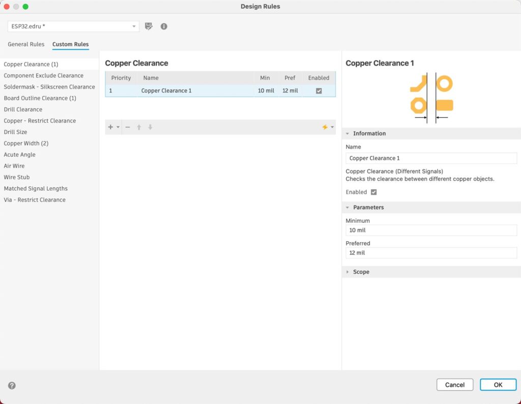
Currently, when manually routing or using quick route tools, all traces will maintain a clearance of 12 mils between traces with different names. The assigned clearance value will be used for specific constraints that apply only to a particular signal on a specific layer. This is when the Rule Scopes become very important and empowering.
“The Scope Option allows users to apply design rules selectively to different parts of the project. Rather than using rules across the entire board, you can target specific layers, components, or nets. This is particularly useful for complex designs where different parts of the PCB require different sets of rules due to differing operational demands (e.g., power traces vs. signal traces). This flexibility ensures that each part of the design is optimized for its specific function, improving overall performance and manufacturability.”
– Pieter Jan Vademaele
Sr. Software Engineer Manager & Architect
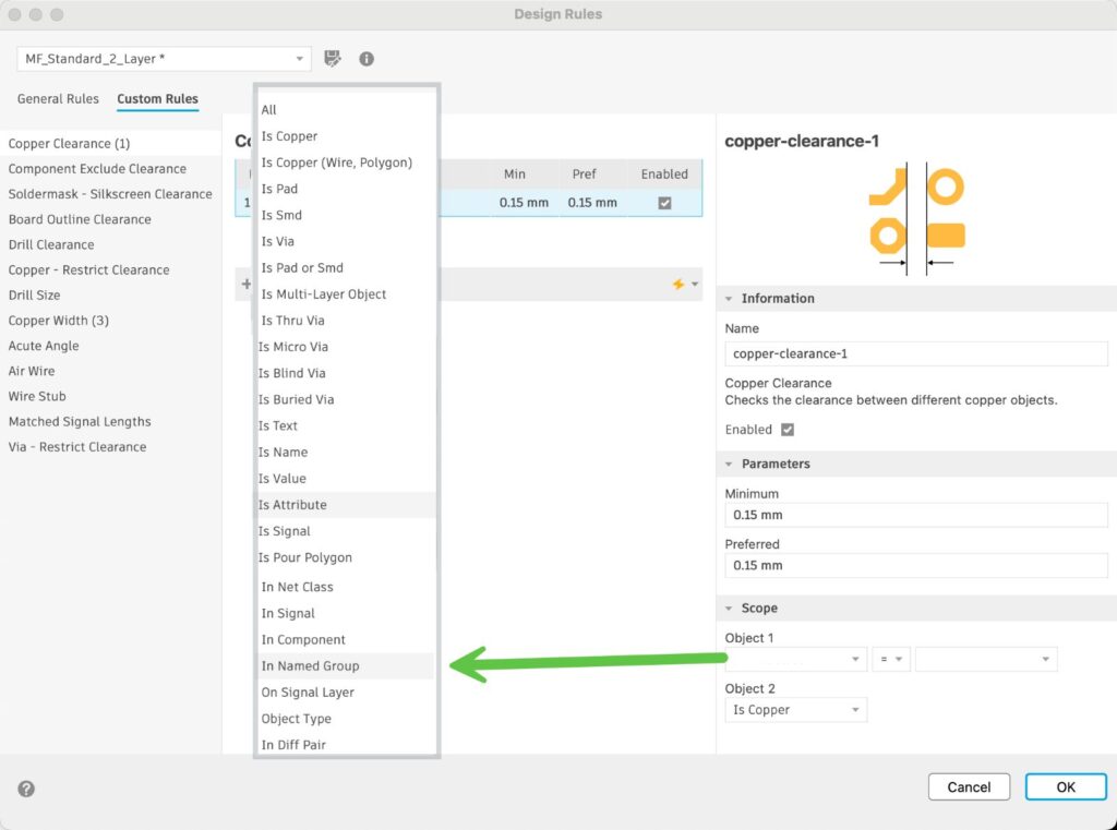
Initially, let’s go ahead and define the scope constraint for the first object. There are many options that can be used from specific signals to net classes and so much more. For this example, the first object’s scope will be set to the signal RXD0. The idea is that RXDO signal will maintain a clearance of 12 mil from V_NIOI2C only on layers 2 and 3. On any other layer it will follow the DRC General Rules Criteria.
The Object scope selection is extensive since you can select Net Classes, Via, polygons, copper, layers, components, and more. This flexibility will allow you to create the rules for PCB function and manufacturability early in the design stage.
After selecting Copper Width from Custom Rules (1), three rules—A, B, and C—were created to define different minimum width preferences for signal VBAT on various layers. Please notice that “A” sets the minimum of 20 mils for VBAT traces on the bottom layer, while VBAT on layer two is expected to have a minimum of 15 mils while traces on the top layer for VBAT will have a Preferred width of 10 mills. This is important because of the flexibility now available to define constraints at a much more granular level.
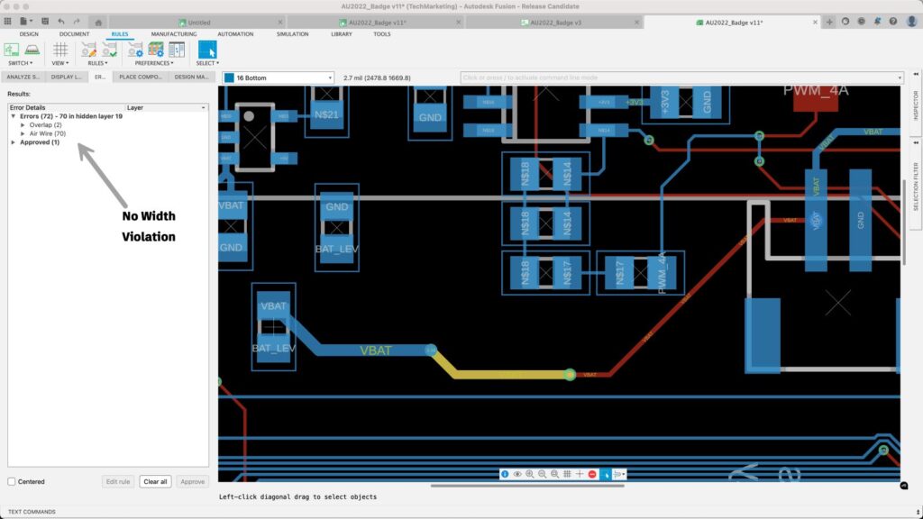
The range of wire width used for VBAT is quite significant but notice that no errors have been generated since all respective wire widths are followed according to the defined Custom Rules.
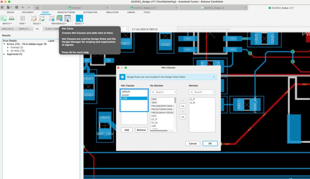
Traditionally, Net Classes were an established method of constraining our traditional global constraints system. With the new engine and interface, we now only use NET Classes to create a set of signals requiring similar constraints. The members of the ‘USB’ NET Class are a differential pair of traces called U_P and U_N. With the Class created and members assigned to it, let’s see how we can work with them.
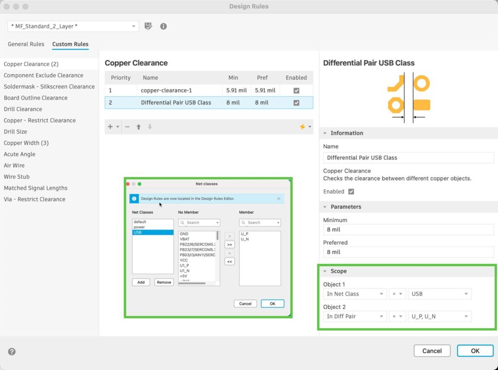
You can now select the Net Class and/or Differential Pair as objects. This allows you to define rules between Net Classes or among Differential pairs.
Another good example is power; commonly, there will be a class called power in which GND, and other voltages will be assigned. With the Custom Design Rule settings, you can now assign the net class as an object scope with other net classes, signals, components, polygons, and whatever else is needed to achieve the correct design function.
By leveraging Global Settings, General Rules, and Custom Rules, along with the Rule Scopes, you can:
Fusion DRC tools aim to bridge the gap between design and manufacturability, offering a set of constraints that efficiently control every aspect of PCB design.

The new design rule preference system in Fusion Electronics Workspace is a game-changer for the electronics design industry. By empowering designers and engineers with unparalleled control over their design parameters, Fusion Electronics Workspace is redefining what’s possible in electronics design. Embrace the future of design with Fusion Electronics Workspace and unlock your full creative potential.
By clicking subscribe, I agree to receive the Fusion newsletter and acknowledge the Autodesk Privacy Statement.
Success!
May we collect and use your data?
Learn more about the Third Party Services we use and our Privacy Statement.May we collect and use your data to tailor your experience?
Explore the benefits of a customized experience by managing your privacy settings for this site or visit our Privacy Statement to learn more about your options.