The Top 10 PCB Component Placement Tips for the PCB Beginner
PCB design is both an art and a science. There’s a ton of technical know-how and measurements to consider when dealing with trace widths, layer stackups, schematics, etc. But then you get to the artistic side of PCB design with component placement, and this is where things get interesting.
The truth is, there is no “right” way to place components, and this freedom is ultimately what makes the PCB layout process so dang fulfilling and creative. It’s all up to you and what you want to design. That’s not to say that you can do whatever you want. There’s still the humbling reality that the digital design you create needs to be manufacturable in its physical form, which is why you’ll want to follow the 10 tips below to make the most of your component placement flow.
What’s So Important About Component Placement?
There’s a common saying that goes something like this – PCB design is 90% placement and 10% routing. This is entirely accurate. Taking the time to precisely place your components will make your life a whole lot easier when it comes time to route everything, while also giving your board its best electrical performance. But what happen if you just slap your components down without care?
- Hours Wasted. You’ll likely create a nightmare for yourself when you find out that some of your parts don’t even have enough space to be routed because you packed them too close together. The worst component placement jobs can lead to an entire board that needs to be started again from scratch.
- Busted Boards. Let’s say you do manage to place down some components and traces and ship your files off to your manufacturer. Next thing you know you might get a board back, that doesn’t work because your parts weren’t soldered correctly (more on this later).
- Ugly Aesthetics. Let’s face it, as engineers we love symmetry and precision, and there’s nothing more unsettling than seeing a board that wasn’t given some proper love and care during its component placement. It’s just plain lazy.
Make sense? Here’s the real kicker – there’s no universally “right” way to do it. Give a schematic to 100 different engineers, and you’ll likely get 100 different layouts back. This is why the PCB layout process is viewed as an artistic process.
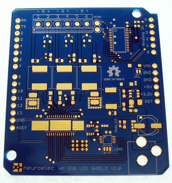
The artistry and elegance of a carefully thought out PCB is a sight to behold. The symmetry, the part placement, so good! (Image source)
Not a fan of all the vague ideas of “right” and “wrong”? Here’s a hint to see if you’re on track with your component placement. After throwing down all of your parts, crank on the autorouter in Autodesk EAGLE. If you don’t get at least an 85% completion rating, then this is a good sign you need to spend some more time on your component placement.
Now that we’ve got the Why out of the way let’s move on to some practical tips you can use in your first design project!
Tip #1 – Understand Your Mechanical Constraints
Before you ever place a part down, you’ll want to know exactly where your mounting holes and edge connectors go and what kind of mechanical enclosure to fit your board.
Why?
Understanding these variables will affect both the size and shape of your board. We’ve seen many engineers design a board that doesn’t fit its enclosure, only to spend hours reworking their entire design again.
You can do yourself a favor by plugging in clearance requirements for your mounting holes in your design rules before beginning a component placement process. This will let you focus on the creative stuff while not worrying about your mechanical constraints.
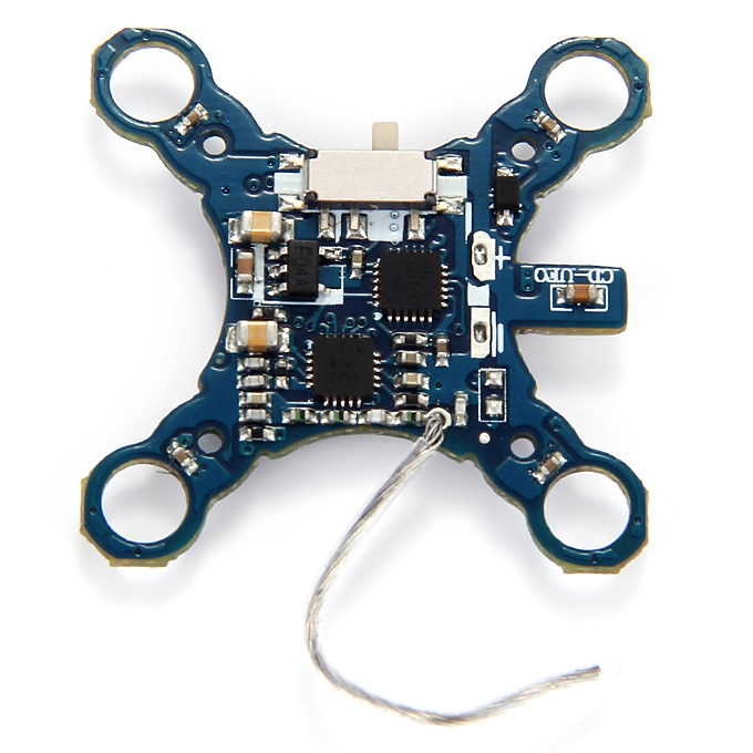
Drones and other flexible and wearable technologies require some interesting board shapes to fit into enclosures. Here’s an example of a PCB receiver for a mini drone. (Image source)
Tip #2 – Understand Your Assembly Constraints
Again, before you ever place a part down, you’ll want to understand a few pieces of information from your manufacturer, including:
- How is your board going to be assembled and tested?
- Will you need to add any clearances to your board for v-scoring?
- How are your components going to be assembled, by wave soldering, selective soldering, or hand soldering?
Why?
How your board is manufactured will ultimately determine what kind of space you have to work with during your component placement process. For example, if your board is going to be assembled along a conveyor belt, then you’ll want to keep parts away from the edge of your board to prevent any damage during assembly and processing.
If your manufacturer uses a pallet array system to fabricate and assemble your board, then you’ll be safe to use the full area of your board when placing parts. However, if you do need to avoid placing components on the edge of your board because of assembly restrictions then make sure that all of your parts and traces are at least 20 mils away from the edge of your PCB.

An example of a PCB panel, which gets snapped off after the board is complete. Notice how in this assembly process components can come to the edge of the board. (Image source)
Tip #3 – Give your Integrated Circuits (ICs) Room to Breathe
Always try to leave at least 0.3500” – 0.5000” of spacing between each integrated circuit (IC) on your board. For larger ICs leave even more space.
Why?
Integrated circuits ship with a ton of pins for various connections and the worst mistake that beginner designers always make is placing their ICs too close together. What happens when you do this? You’ll likely run out of space when it comes time to route all of the pins on your IC, and you’ll have to move a bunch of things around, wasting hours or days of work.
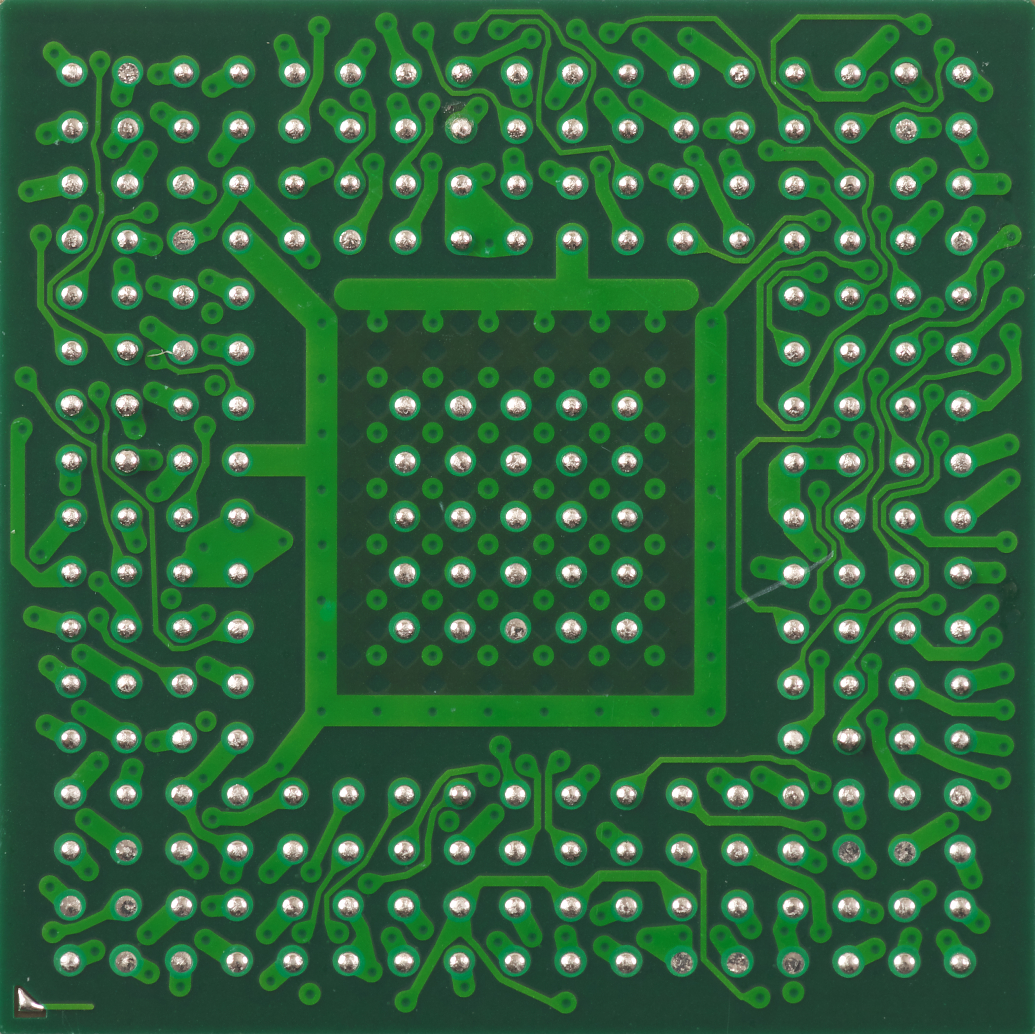
Some integrated circuits like this Ball Grid Array (BGA) have a ton of nets to connect, no wonder why they need some space to breathe!
Tip #4 – Keep Similar Components in the Same Direction
For groups of similar components, take the time to orient all of them in the same direction in evenly arranged rows or columns.
Why?
Doing this will make it easy for your manufacturer to install, inspect and test all of your placed parts. This ends up being critical if you’re working with Surface Mount components or SMDs which use a wave soldering process. During this wave soldering process, the bottom of your board will move over a molten wave of solder, and when the wave touches any exposed metal piece, it gets coated with solder.
So when you have two exposed metal surfaces like a lead in a hole, as the wave solder passes over a solder joint will get formed, allowing an electrical connection to flow between your board and component. If these connections don’t get soldered correctly, then you’ll wind up with a board that has a bunch of shorts or open circuits.
There’s an example below of this wave soldering process in action. Here we have components arranged in the same orientation. When this board passes through the wave soldering oven, then every part will get soldered evenly.
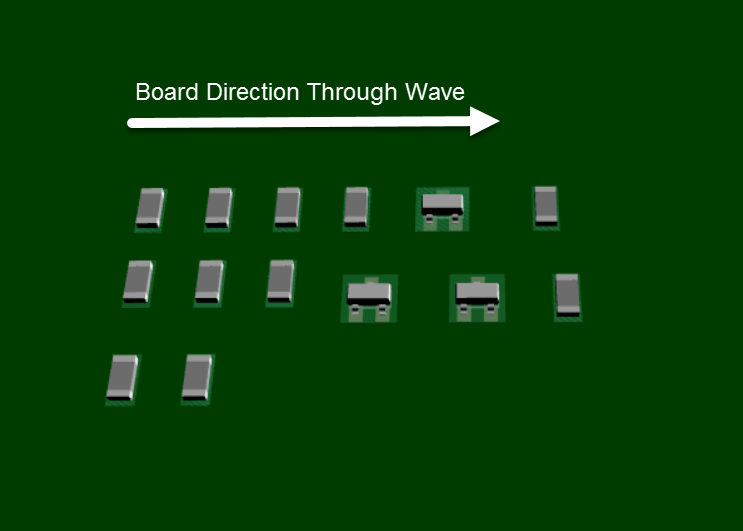
An example of an excellent component placement technique with parts all oriented in the same direction for an even soldering process.
However, below we have components that are all over the place in different orientations. This placement is likely going to result in some terminations that don’t get soldered entirely. And if you happen to have small components sitting behind taller components you’ll also end up creating a “shadow” effect that could cause the small parts to get improperly soldered.
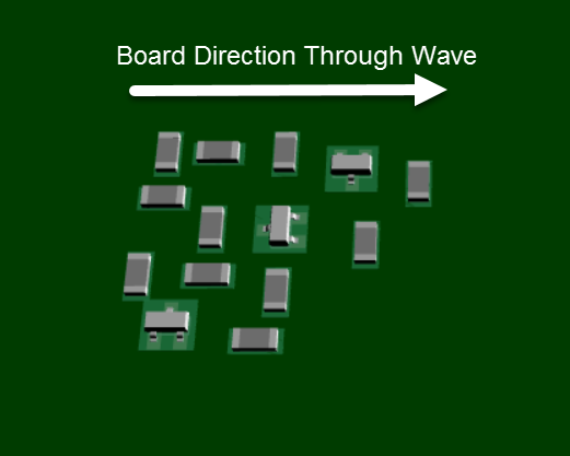
An example of a not-so-great component placement technique. These parts oriented all over the place likely won’t be soldered completely.
Tip #5 – Group Your Parts to Minimize Connection Paths
When you place your components minimize any intersecting and criss-cross of connection paths.
Why?
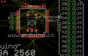
When you transform a schematic into a PCB layout in Autodesk EAGLE, you’ll notice that each of your parts has a very thin line that connects to another part. These lines are called airwires, and you’ll also hear them referred to as a ratsnest in other PCB design tools. These are all the connection points between parts that you created with your schematic design.
 |
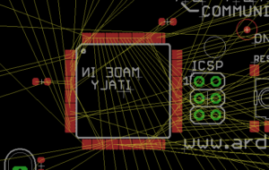 |
By minimizing the amount of intersections and criss-cross of connection paths, you’ll make your routing job a whole lot easier and straightforward. Autodesk EAGLE has a handy Ratsnest ![]() tool on the left-hand side of the interface that makes it easy to recalculate your airwires as your move parts around. Be sure to keep selecting this button as you place parts to keep track of your progress.
tool on the left-hand side of the interface that makes it easy to recalculate your airwires as your move parts around. Be sure to keep selecting this button as you place parts to keep track of your progress.
Tip #6 – Place All of Your Edge Components First
First place all of the components that can’t be moved due to a mechanical enclosure, like connectors, switches, jacks, USB ports, etc…
Why?
The placement of these components is all set in stone and are typically out of your control if you are working with a mechanical designer. And by placing these edge components first, you’ll give yourself a great starting point for how your board layout needs to unfold to accommodate all of your input and output connections. After locking these edge components into place, you can start on the real fun and creative work with your interior parts.
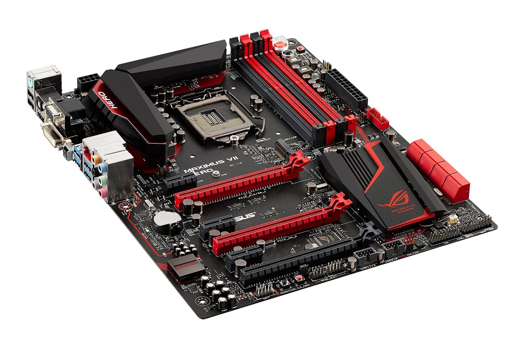
Motherboards are a great example of how connectors are placed on the edge of the board layout. (Image source)
Tip #7 – Avoid Overlapping Any Parts
Never, ever cut corners if you’re working with a small board size by overlapping parts, being either the pad or the part outline. Keep at least 40 mils of space between all of your parts.
Why?
Each footprint that you place on your PCB contains a set of copper pads that will have an electric connection. If you overlap two parts and the pads touch in even the slightest amount, then you’ll allow a stream of electricity to cross between components, resulting in some unintended short circuits.
Plus, when you give yourself space between parts during your placement process, you’ll also have a much easier time routing all of your copper traces. Don’t forget about those vias holes too! Those green rings are just a bunch of exposed copper that would love to short circuit your board if they aren’t given enough space.
Tip #8 – Keep Your Parts On One Layer
If you’re working with a simple 2 layer board, then we always recommend placing all of your parts on the top layer.
Why?
Manufacturing a physical PCB is a time-consuming process, and an expensive one if you end up placing components on the top and bottom layers of your board. Here’s why – in the assembly process your SMD components will be placed on your PCB through a rapid-fire pick-and-place machine.
This process is straightforward and will require only one pass through the pick-and-place machine if you put all of your components on the top layer of your board. But if you start placing parts on your bottom layer then you’ll require yet another pass through the pick-and-place machine, resulting in some unnecessary manufacturing costs.
Tip #9 – Keep IC Pins and Polarized Components in the Same Direction
Every integrated circuit (IC) has an identifier that shows where pin 1 is, and you can take advantage of this by always aligning pin 1 on all of your ICs in the same direction.
The same goes for polarized components, make sure that the positive leads are all placed in the same direction.
Why?
By placing all of your ICs in the same direction then you’ll ensure that no mistakes are made when it’s time to solder and inspect your board. Imagine having to assemble a board where every IC was facing the wrong direction that would be a disaster!
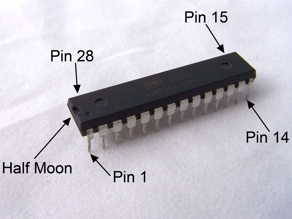
All integrated circuits have a dot to indicate their first pin. Orienting all of your ICs the same direction makes it easy to solder and inspect your board.
Tip #10 – Design Your PCB Layout Like Your Schematic
Place components in logical groups on your PCB layout just like you did with your schematic design.
Why?
You’ll save a ton of time in the process and make your design easy to compare between schematic and PCB layout. This will also have the benefit of minimizing the length of traces since the parts you’re placing are already logically grouped together based on your schematic.
For example, if you have a big microcontroller to place, you’ll want to place that part first, then all of the supporting components like resistors and capacitors around it. This will make it easy to route your IC and all connected components with trace lengths that are as short as possible.
Contained Creativity
The best PCB layouts started on a foundation of great component placement, and there’s no reason to rush through this process. If you find yourself spending 90% of your time placing parts, then you’re doing something right, keep it up! This process is a rewarding creative endeavor, and probably one of the most challenging aspects of the PCB design process that you’ll wrestle with, but it’s totally worth it. At the end of the day, taking the time to place your parts efficiently will get you a board back from manufacturing that works right out of the box. And that’s every engineer’s favorite moment.
Ready to start your first PCB design project? Subscribe to Autodesk EAGLE today!
