From Subtractive to Additive: PCB Manufacturing is Heading to Your Desktop
3D printing is booming for businesses and hobbyists. In the 2017 State of 3D Printing report from Sculpteo, it reports that 57% of all 3D printing work is done in the first stages of a new product development. What does this mean for businesses and the engineers behind it? Ideas can be tested faster, designs can be refined without the heavy costs of traditional manufacturing, and consumers win with more innovative products. While 3D printing has hold of mechanical engineering, architecture, and product design, we have to ask, what about us in electronics?
Subtractive vs. Additive in Electronics Manufacturing
3D printing and additive manufacturing for electronics is still in its infancy, but not because of a lack of interest. The problem has more to do with limitations in materials, and the simple yet challenging question of you how print all of the various layers, materials, and components found in today’s densely packed PCBs?
These days, PCBs are still manufactured in a traditional subtractive process. Here, the entire surface of a PCB is plated with copper and the areas that don’t require copper are etched away from the board. It’s like taking a piece of wood and cutting it down to get your required shape and structure. There’s a lot of waste in the process.
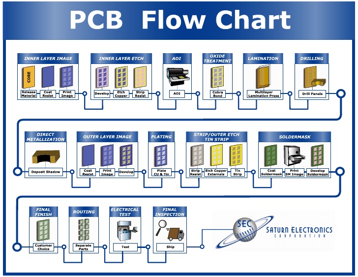
With additive manufacturing, the process works in reverse. Instead of starting with more material than you need, you build up materials as you need it. For example, rather than etching away copper on an FR4 substrate, in an additive process you’ll start with a thin FR4 substrate and then add copper traces with conductive ink. This additive approach has some serious implications for both engineers and manufacturers, including:
Freedom to Design and Innovate
As engineers, we’re all accustomed to redesigns and respins, which typically comes later in the design process than we’d like. With additive manufacturing machinery deployed in-house, engineers can enjoy the creative freedom to make changes to a design without traditional time or cost penalties. Imagine being able to iterate on a design and create a prototype on your desktop without waiting around for your fab house to send boards back.
Less Waste and Costs
Additive manufacturing generates way less waste than traditional subtractive methods. Because materials are being added layer by layer, machines are only using materials that are needed for the task at hand without any of the added waste of removing materials. It has been found that additive manufacturing can reduce material costs and waste by up to 90 percent.
Protected Intellectual Property
With in-house additive manufacturing businesses no longer need to ship off their intellectual property to a third-party. This keeps the risk of an IP exposure in-house, and allows businesses to rapidly prototype and iterate on ideas while keeping development costs low.

The benefits of additive manufacturing also extend to the PCB itself. Circuit boards made with an additive manufacturing process provide:
- A higher board density with traces packed into smaller areas.
- Consistent trace definitions and trace widths which can improve signal integrity.
- Thinner and more flexible circuits which are ideal for wearable applications.
- More consistent electrical and mechanical performance.
- Greater quality control in electronics with flex/rigid circuitry and varied trace thicknesses.
Additive Manufacturing On Your Desktop
There are two additive manufacturing solutions for electronics – 3D printing and 2D printing. In 3D printing, circuit boards are printed from scratch, layer by layer, with a variety of conductive inks, gels, and substrates that are manufactured at the nanoparticle level. 3D printing for PCBs is still very new, largely because of material complexity and extrusion requirements.
There’s also an issue with design software compatibility. We all rely on Gerber files to communicate designs to manufacturing, but doing so presents a 2D perspective of our board. The question then is how you convert these 2D files into 3D printable files, which need to define thicknesses for substrates, via and hole depth, trace dimensions, and more? Design software and manufacturing outputs that meet these unique requirements are still not here.
On the other side of additive manufacturing, we have 2D inkjet-style printing. These machines use a printhead that prints conductive traces on a flat horizontal substrate. This is an ideal situation for printing 2 layer boards for quick prototyping.
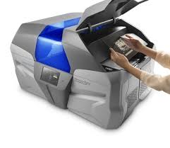
One of the leaders in the 2D PCB printing space is Voltera, which makes the V-One PCB Printer. This printer can produce double-sided PCB prototypes, dispense solder paste, and even acts as a reflow oven for component assembly.
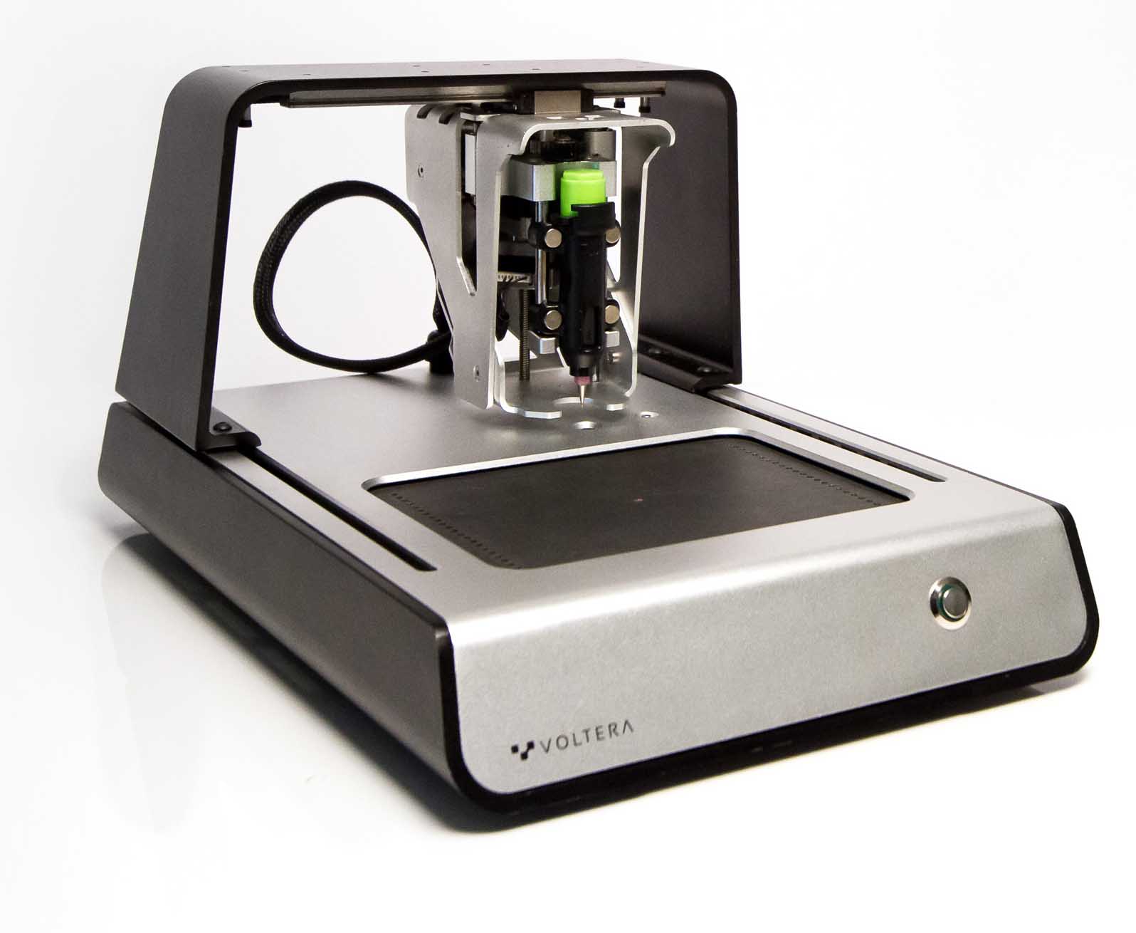
Consider your current workflow for creating a prototype. You have to send off your design files to a fab house and wait days or even weeks to get your boards back. With the Voltera V-One PCB Printer, you can experiment and prototype new ideas in hours instead of days. This has the potential to change the way we as engineers approach our design process, just consider:
- Having more time to quickly experiment with new ideas when you aren’t tied down to a fab house for prototypes.
- Being able to get your product out to market faster by iterating early and addressing risk points at the beginning of your design process.
- Understanding the impact of design changes before they reach the manufacturing floor by identifying problems in a prototype.
Sound like a better world of engineering? Voltera seamlessly integrates with your existing design process and allows you to:
- Print your own circuit boards. Go from prototype to production for two layer circuit boards right from your desk. The ink used in the V-One is 90% silver and perfect for digital and low power applications, even at frequencies up to 5 GHz.
- Focus on designing, not soldering. No more messing with solder paste and stencils just to produce a prototype. Solder is applied by the machine, and a 550W heating platform reaches reflow temperatures in under a minute.
- Integrate rapid prototyping into your design process. The Voltera software allows you to import existing CAM files from EAGLE. Once your design is loaded into the software, it’s simply a matter of identifying 2 features on your board for alignment and your work is done.
For those concerned about 2D PCB printers meeting the needs of modern electronics, worry not. Voltera’s machine can handle 0402 package sizes and 8 mil traces. Here the full list of V-One specifications.
Voltera Design Blocks for EAGLE
Voltera and EAGLE have teamed up to offer a ton of free design blocks to get your first project started quickly. These include:
Basic Substrates
Use these design blocks when you need to start an electronics project from scratch. There are also included variations for plated clustered and distributed via designs.
- Voltera 2″ x 3″ Substrates
- Voltera 3″ x 4″ Substrates
- Voltera 4″ x 5″ Substrates
- Voltera USB Templates
- Voltera Pre-Plated Clustered Vias Templates
- Voltera Pre-Plated Distributed Vias Templates
Design Platform Substrates
Use these design blocks when you need to expand an existing development platform for your Arduino, Raspberry Pi, or Particle Photon.
- Voltera Raspberry Pi B+ Templates
- Voltera Arduino Mega Templates
- Voltera Arduino Uno Templates
- Voltera Particle Photon Templates
PCB Manufacturing On Your Desktop
3D PCB printing still has a long way to go for the electronics manufacturing industry as we overcome material challenges and unique extrusions. However, for today’s PCB designer, prototyping and iterating on new ideas has never been easier thanks to affordable 2D PCB printing technologies. The Voltera V-One PCB Printer makes it easy to design, prototype, and assemble double sided PCBs on your schedule, right from your desk.
Ready to get your hands on a Voltera V-One PCB Printer? Check out their website for more information.
Already have the V-One? Be sure to download the free Voltera Design Blocks for EAGLE!