& Construction

Integrated BIM tools, including Revit, AutoCAD, and Civil 3D
& Manufacturing

Professional CAD/CAM tools built on Inventor and AutoCAD
1 min read
Welcome to the first installment of our Everyday App Note Series! Today’s application note comes from Texas Instruments, one of the leading experts on high-speed design. They’ve dug deep to uncover solutions for timing errors during high-speed Analog-to-Digital Conversion (ADC) when using Low Voltage Differential Signaling (LVDS) and a Field Programmable Gate Array (FPGA).

The LVDS standard does not define any connectors and protocols, which makes it easily adaptable into a variety of high-speed applications. This app note is perfect for any designer troubleshooting timing errors during high-speed analog-to-digital conversion with an LVDS data interface and an FPGA.
LVDS is one of the most popular differential signaling standards for electronics design and offers an ideal interface between an ADC and FPGA. If you’re battling timing errors using single-ended signaling schemes like Complementary Metal-Oxide-Semiconductor (CMOS), then this app note is worth your time.

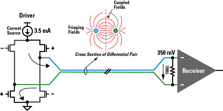
It’s a well-known fact that differential signaling with LVDS greatly reduces noise on high-speed layouts than single-ended schemes like CMOS. By using two wires with opposite current and voltage swings in a differential signal, you get several benefits, including:
Data from two differential signals that aren’t captured at the same time by an LVDS receiver presents signal timing and noise problems for your high-speed layout. This marginal capturing issue can only be solved with one of two methods that this app note discusses in detail:
There are a lot more details inside. Learn how to avoid timing errors by downloading this application note from Texas Instruments now!
By clicking subscribe, I agree to receive the Fusion newsletter and acknowledge the Autodesk Privacy Statement.
Success!
May we collect and use your data?
Learn more about the Third Party Services we use and our Privacy Statement.May we collect and use your data to tailor your experience?
Explore the benefits of a customized experience by managing your privacy settings for this site or visit our Privacy Statement to learn more about your options.