Everyday App Note: How to Design a Buck Converter Circuit with This Layout Strategy
Buck Converters are an ideal solution for regulating a DC output voltage to be lower than a DC input voltage. These DC-to-DC converter circuits are much more power efficient than a linear regulator and are perfect when you need to convert mains into lower voltages. Today’s Everyday App Note from Rohm Semiconductor will walk you through a precise layout strategy to successfully design a buck converter circuit.

Process at a Glance
The layout process for a Buck Converter circuit is just as important as the rest of your circuit design. Poor converter layouts can often result in increased noise that affects your output switching signal, reduced efficiency of your regulator, and poor switching power supply stability.
To ensure a successful layout process, Rohm has assembled a layout strategy that takes you from beginning to finish to design a Buck Converter circuit. These steps include:
- Placing input capacitor(s) and a free-wheel diode for core functionality
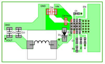
These two components need to be placed on the same layer as the IC terminal. In a small current power supply, a single ceramic capacitor can function as both an input and bypass capacitor. For higher current supplies two capacitors will be required as shown below:

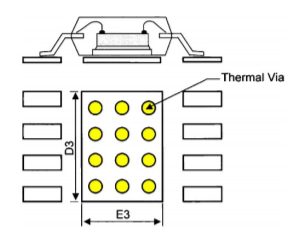
- Adding thermal vias for improved heat dissipation
For smaller PCB layouts, the size of the copper area on a board doesn’t provide adequate heat dissipation. To send heat to the bottom layer of a board and reduce heat resistance you can use a thermal via as shown below:

- Placing an inductor close to IC to minimize radiation noise
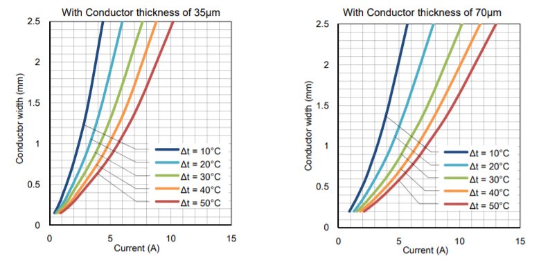
An inductor needs to be placed close to your IC to reduce radiation noise from the switching node. You need to be mindful of trace width between these two components. For example, temperatures can be reduced 20°C by maintaining a 0.53mm conductor width for 2A of current flowing through a trace. The graph below shows a comparison of temperature fluctuations based on conductor thickness.

- Placing an output capacitor close to the inductor
An output capacitor should be placed close to the inductor to help smooth output current. The input and output capacitor requires a distance of at least 1 cm from each other. Otherwise, noise from the input can propagate to the output. - Maintaining feedback distance from noisy areas
If the feedback trace gets coupled with noise from the inductor or diode, voltage errors and unstable performance will result. The image below shows the points in your circuit to be mindful of when routing a feedback path.

Download This Layout Strategy Now
Power supply reliability is no joke, and careful consideration needs to be made to the placement of each component and wire. This application note will walk you through all of the critical components to design a Buck Converter circuit from beginning to finish.
Download the PCB Layout Techniques of Buck Converter App Note now!