This article explores the various design for manufacturing (DFM) considerations you should make when designing your next PCB.

In the realm of electronics, designing a printed circuit board (PCB) is a critical aspect. However, crafting the perfect PCB is not just about the design; it’s also about considering the manufacturing process. This comprehensive guide will explore the various Design for Manufacturing considerations you should make when designing your next PCB. Understanding these concepts will help you avoid common mistakes and ensure a successful and efficient manufacturing process.
Understanding Design for Manufacturing (DFM)
Design for Manufacturing, or DFM, is designing products with the manufacturing process in mind. It is the amalgamation of two methodologies: design for fabrication (DFF) and design for assembly (DFA). DFF and DFA ensure that products are designed in a way that they can be manufactured and assembled efficiently and quickly.
DFM is intended to challenge the design stage at all levels. It checks the accuracy of the design at the system level, sub-system level, and component level. By following proper DFM processes, potential problems associated with PCB design can be mitigated, and a smooth fabrication and assembly process can be ensured.
The importance of DFM in PCB design
Designing with a focus on manufacturing requires a big-picture approach to PCB construction. Implementing Design for Manufacturing in your design process leads to several advantages:
- Fewer Iterations: DFM reduces the number of redesigns by considering all the limitations and challenges of the manufacturing process from the start.
- Shortened Time-to-Market: DFM decreases lead time and product time-to-market by reducing resource needs and eliminating redesigns and iterations.
- Quality Products: DFM improves the quality and performance of products by providing superior PCBs that meet all specifications and standards.
How Design for Manufacturing enhances product quality

Design for Manufacturing improves the quality and performance of products by providing superior PCBs that meet all specifications and standards and overcome limitations and challenges that could reduce the quality of the PCB. By applying DFM principles, high-performance yet low-cost products can be ensured.
The three phases of the DFM process
The DFM process in PCB design has three main phases:
- Design Phase: This phase focuses on developing a PCB layout design with the correct footprint and component packaging.
- Component Placement Phase: This phase focuses on component placement by following the placement rules.
- Wire Routing Phase: This phase focuses on properly routing wires by considering wiring standards.
By following these three phases of the DFM process, manufacturing can accelerate and enjoy benefits such as minimal material wastage, increased productivity, reduced production time, and scaled-up production—all at a reduced cost.
5 Design for Manufacturing tips for PCB design
1. Focus on material considerations
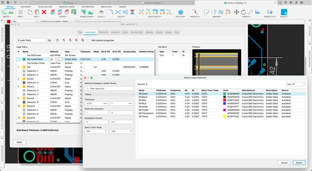
One of the primary areas to focus on when designing a PCB is material considerations. For instance, you need to know the layer arrangement and material properties before creating traces for digital buses or any controlled impedance traces. Using copper weights available on your fabricator’s material set is crucial. If you estimate the copper weight and trace width you need for a specific current density (such as on power rails), you should ensure to specify the required weight when determining the stackup with your fabricator.
2. Understand fabrication limits
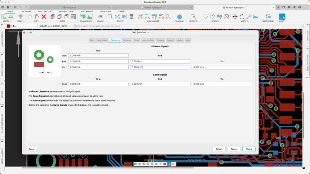
In the context of PCB design, fabrication limits refer to feature sizes and spacing in a PCB layout. When you start a new PCB layout, your ECAD software will apply default clearance rules. It’s common to only ignore these values after programming the correct clearance values before creating the layout. This could result in elements being placed too close together, making the board impossible to manufacture. To avoid this, you should get your fabricator’s limits before you start placement and program these values as design rules into your PCB project.
3. Follow component placement best practices
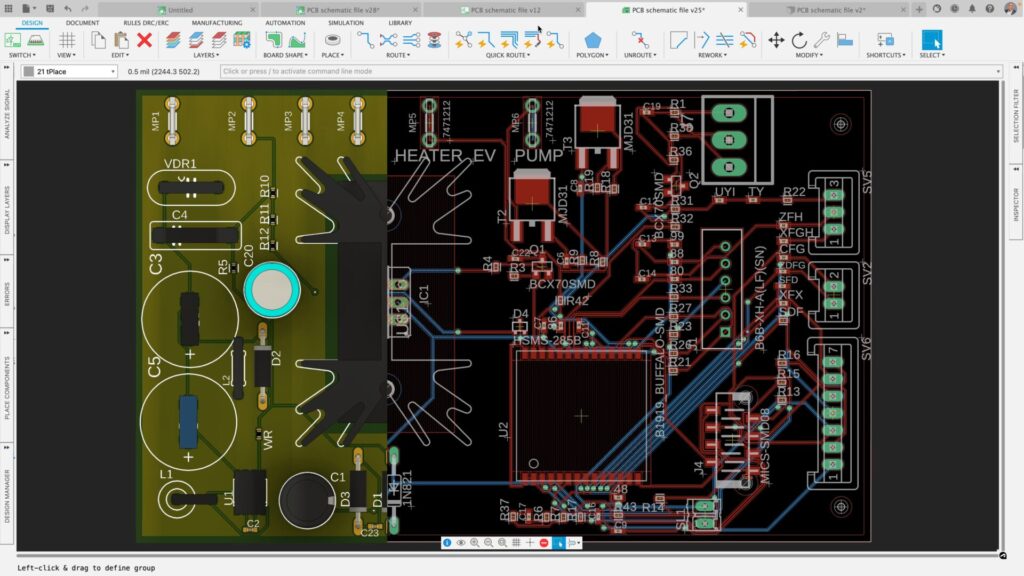
Component placement is a critical aspect of PCB design and significantly impacts the manufacturing process. A poorly placed component can lead to manufacturing issues, increased costs, and reduced product quality. Therefore, following best practices for component placement is essential to ensure a smooth and efficient manufacturing process.
4. Ensure efficient wire routing
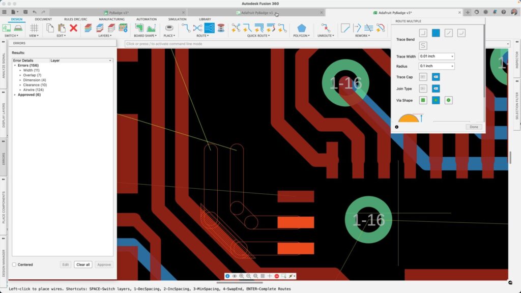
Wire routing is another essential aspect of PCB design that can significantly impact the manufacturing process. Proper wire routing ensures that the signals on the PCB can travel from one point to another without interference. By considering wiring standards and following best practices for wire routing, you can optimize the performance of your PCB and streamline the manufacturing process.
5. Choose the right manufacturer
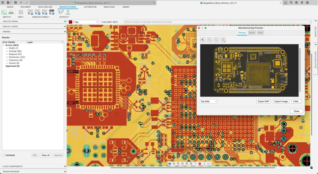
Choosing the proper manufacturer is crucial for guaranteeing a smooth production process. Designers must find a PCB manufacturing partner in the right location, with a good reputation, comprehensive customer support, and the capabilities to produce high-quality products at high volume. Once a manufacturer is selected, designers can work directly with that firm to ensure their designs are manufacturable. This allows them to update designs early instead of further in the process when such an issue is inevitably more costly and time-consuming.
Design for manufacturing collaboration: best practices

A digital thread between design and manufacturing enables teams to minimize the respins that often happen between the design and manufacturing teams. Simplifying the transition to manufacturing requires sharing a complete understanding of the product and enabling early downstream access to the data. Running a manufacturability analysis before sending your design to your manufacturer quickly identifies potential manufacturing issues, minimizing respins and eliminating the possibility of undesired changes made to the design by manufacturing errors.
Adhering to Design for Manufacturing considerations when creating your next PCB is vital. By keeping these primary concepts in mind and avoiding common mistakes, you can ensure an efficient and successful manufacturing process. Remember: designing the electronics of any product requires following manufacturing guidelines. The goal is to get it done right with fewer respins. So, apply these insights in your PCB design process and watch your manufacturing efficiency soar.