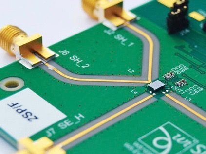
Moisture, humidity, dust? No problem! This article covers the main considerations you need to make when designing PCBs that will live in harsh environments. High temperatures will be no match for your next PCB.
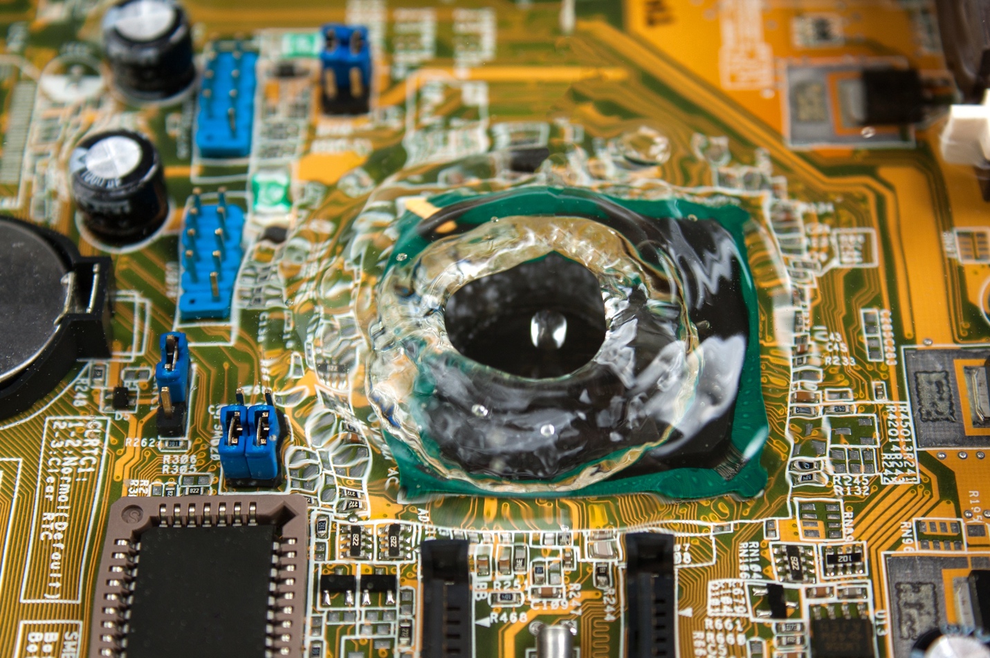
If you investigate any modern electronic device, you will notice that the PCB is an essential part of the system. PCB stands for printed circuit board, which means the circuit is printed on non-conductive material. They’re generally made of water-resistant FR-4 fiberglass materials that can withstand high temperatures and provide insulation between copper layers that minimizes interference and supports good signal integrity. These features make FR-4 fiberglass a perfect material for general-purpose PCBs. As a result, they’re widely used in most consumer electronics products.
However, these characteristics do have limitations. For example, depending your PCB’s intended use cases, you may need a circuit to withstand some harsh environments. To make the circuit functional and fully operational in these extreme conditions, you’ll need to consider a few more factors.
Harsh Environments Examples
- Extreme temperatures, both hot and cold
- Temperature or humidity fluctuations
- Rain/moist environments
- Dirt, dust or other contaminators
- Power surges, either natural (i.e., lightning) or human-made
- Electrostatic or electromagnetic interferences
Designing a PCB that will withstand harsh environments requires special skills and knowledge to ensure the final product can last longer in such situations. Let’s look at the challenges we’ll face for each condition and how to overcome them.
Temperature
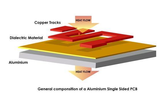
As you already know, any electronic device dissipates some amount of heat while functioning. There are several reasons behind this heat generation. For standard circuits, the amount of heat is not enough to harm the whole circuit. A prevalent way to dissipate heat from a circuit is by adding a copper surface layer to the circuit’s unused part. The FR-4 material is not an excellent conductor of heat, but the copper pour helps the circuit cool down.
This technique only works up to a certain extent, though. If the produced heat is too much, we generally use metal-clad PCBs where an electrically insulated aluminum sheet is used as the PCB base. The aluminum absorbs heat much faster than FR-4 material, it protects PCB components from overheating, and it extends their lifespan. Aluminum PCBs are generally used in making LED light panels.
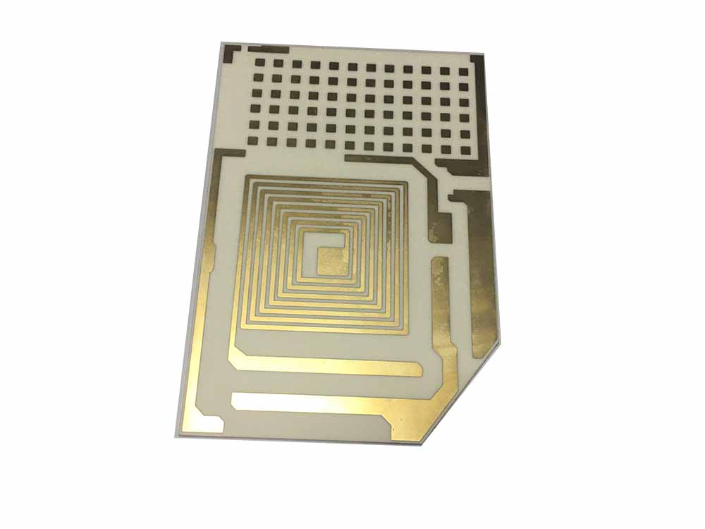
If that isn’t enough, there’s also a ceramic PCB to consider. The PCB’s basis is ceramic and extremely thermally conductive elements such alumina, aluminum nitride, and beryllium oxide (which are frequently coated with immersion gold). This coating can quickly move heat away from hot regions and dissipate it throughout the entire surface.
Ceramic offers a significant advantage over more traditional materials like FR-4 and metal-clad PCB in terms of heat dissipation. The passage of heat through the board is significantly more efficient since the components are directly on the boards with no isolation layer. Furthermore, high operating temperatures (up to 350°C) might harm the ceramic material. It has a very low thermal expansion coefficient (CTE), allowing for additional compatibility options for PCB design.
In general, dealing with an issue at its core is more effective. However, this isn’t always possible. There are several options when dealing with PCB’s that need to operate in extremes temperatures:
- Tighten the operating temperature rating of your product (your product may not need to be designed for temperatures up to +125°C if you specify to users that it must be operated below +85°C).
- Use external heating or cooling units and choose whether heating circuitry, cooling circuitry, or both are required to manage the temperature of the circuit board.
- Design the circuit board with components that can withstand a wide temperature range.
Moisture, Humidity, and Dust
If the PCB will be outside or exposed to nature, it will need to be shielded from natural elements, including water, dirt, and dust. You will harm the circuit or device if no precautions are taken.
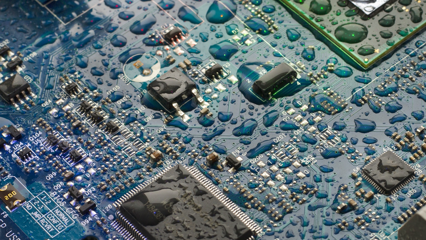
To prevent this, after assembly, spray or ‘paint’ the PCB components with conformal coatings to keep the circuits dry and dust-free.
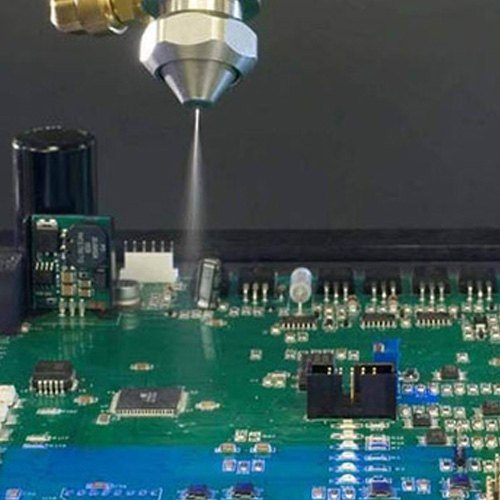
Conformal coating is an option to keep electronic components functioning in less-than-ideal environments. There are four primary types of conformal coatings, each with its advantages and disadvantages.
- Acrylic Resin
- Epoxy Resin
- Silicone Resin
- Parylene
The coating is chosen based on the application and the functional requirements within the application.
High Power Application
As you already know, PCB circuits are made from thin copper traces. These copper traces are rated for low power applications as the current flowing through a conductive material is directly proportional to the width and thickness of the cross-section area of that trace. For general-purpose PCBs, the layer thickness is 1oz/. So, if we need to pass a higher current, we can increase the width of the trace or make the trace multi-layered to increase the cross-sectional area so that it can carry higher currents.
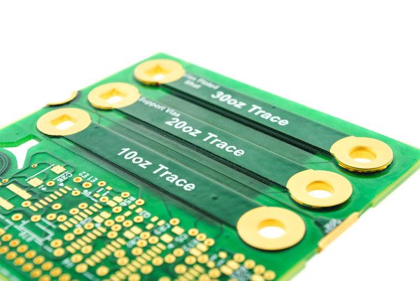
If that’s not an option, then we need to use more copper in the board, and for that, we need to opt for thicker PCB traces so that it can easily handle higher currents.
Signal Interferences
The protection we discussed so far will only protect the PCB against the elements and weather conditions. However, sometimes electromagnetic interference and other forces can generate transients that can destroy components or the whole circuit board. In addition, different types of surges can occur, so it is crucial to understand how to protect your PCBs during the design phase best.
Electrostatic Discharge (ESD) is the most common type of surge. The buildup of charge on the equipment or people near it can produce a surge that damages or destroys semiconductor components. ESD is especially harmful to the most sensitive parts on the PCB, such as the processor and other ICs. It can erase or corrupt memory chips. In addition, it can affect its properties to show false data, or it can ultimately damage the sensors.
To prevent ESD, you should keep the pad separate from the PCB ground so that any shock at the input isn’t immediately routed to every other component on the board. Instead of connecting to the ground, you should use an ESD suppressor at each external connection to protect the board and its sensitive components.
Electrical Fast Transient (EFT) happens when an inductive load is turning on. Inductive loads such as fans and water pumps usually contain a big pile of metal wires wrapped around a non-conductive core to form a big coil or Inductor. These Inductors store energy in their coil and release the power when needed, which can also have damaging effects. The released energy can usually back feed into the controlling circuit. Since the energy has a higher voltage potential than the operating voltage, it can cause severe damage to the circuit.
We can add a Schottky diode to prevent the energy from going back to the circuit (also known as flyback diode), connected across inductive coils to avoid voltage spikes. We can further use optocouplers to provide galvanic insulation between the high side and low side.
Electromagnetic Interference
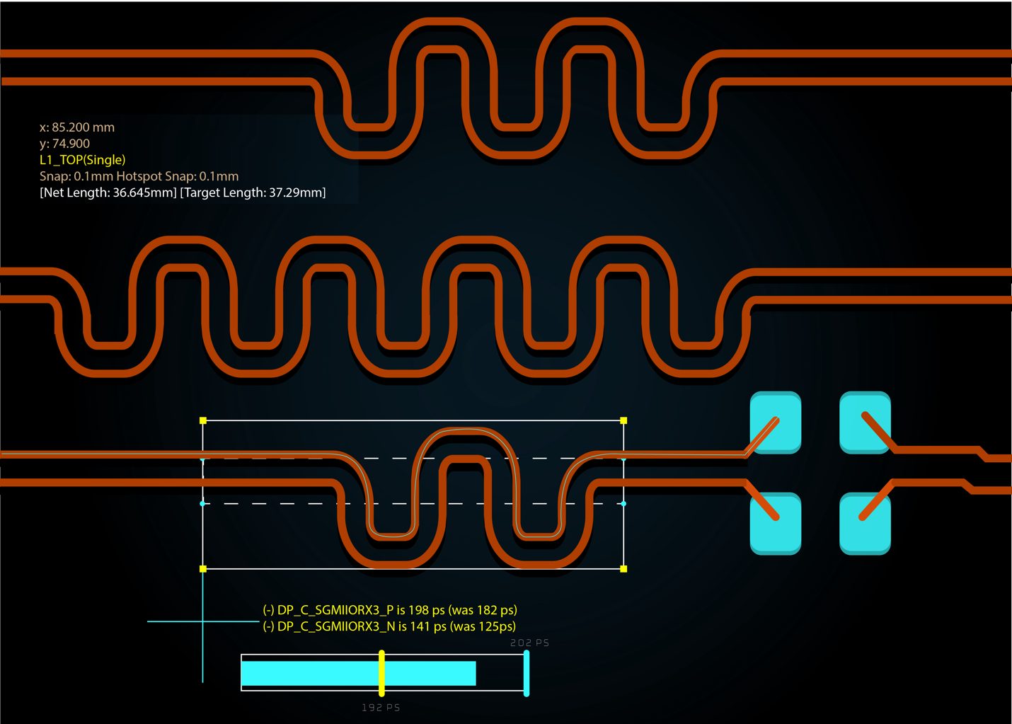
Also known as EMI, an electromagnetic disturbance happens when energy is transmitted through radiation or conduction from one electronic device to another and corrupts the signal quality causing malfunctioning. EMI focuses on the testing requirements and interference between the neighboring equipment. It can occur in any frequency range, especially on analog, RF, or high-speed circuits. To reduce EMI in a PCB, consider these design rules:
- When the signal traces come across any bend or cross or create a large loop within the circuit, they form a fully radiating antenna vulnerable to external noise.
- Having the output traces and input traces for a long-distance creates parallel crosstalk that can be decreased by adding ground planes or increasing distance between lines.
- You should avoid bending the traces at an angle of 90°. The corner should be an arc or with a grade of 45°.
- I always recommend keeping the signal lines as short as possible to reduce the interference signal coupling path. Clock signal lines and sensitive signal lines should always be routed first. Next come high-speed signal lines, and finally, come insignificant signal lines.
- Differential pair routing is a design technique used to create a balanced transmission system. This is done by routing differential (equal and opposite) signal traces together. The signal at the receiving end is interpreted as the difference between the two lines that make up the differential pair.
- And finally, A ground plane with a low inductance value is crucial during PCB designing to mitigate several interference problems. Increasing the ground area on a PCB reduces the ground inductance in the system, hence EM emission and crosstalk.
In addition to these three types of pulses, lightning and other forces can negatively affect electronics integrity. Developing PCB designs that shield against these surges helps maintain circuit integrity and efficiency.
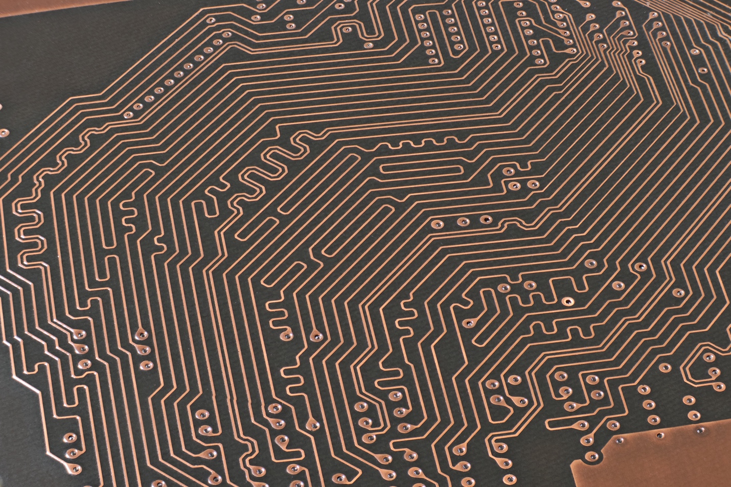
Designing PCBs that can withstand all these harsh environments is not a straightforward task. It requires some advanced knowledge and experience to overcome these challenges. Issues become much more crucial to a product’s viability in extreme adverse settings, such as the cold vacuum of outer space or the heat and dust of the desert. Thus, solutions become more sophisticated from a design standpoint.
The challenge in the design process of PCBs for harsh environments is to design interconnects per the circuit diagram, including all active circuits that will function properly within the limits of any allowable changes in component characteristics.
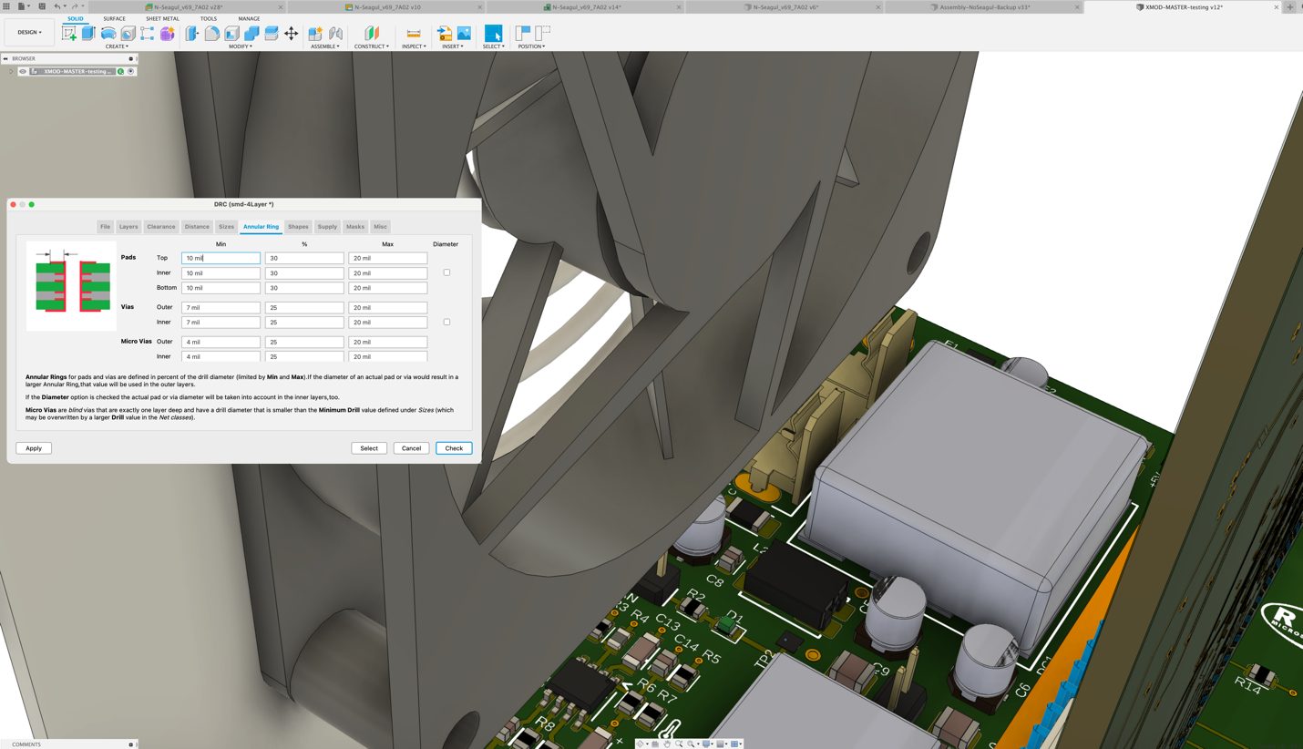
During the initial stages of your design, make sure to consult with your PCB manufacturer to be informed of their recommendations for your design. Many of them conveniently provide a Design Rule file that you can load into Fusion 360. Fusion 360 provides real-time DRC checks during the layout process.
Download Fusion 360 today to experience an integrated electronics design solution.

