PCB Layout Basics Part 3: How to Run a DRC and Add Your Finishing Touches
Welcome back to our PCB Layout Basics Series! If you’ve come this far then all the hard work is already behind you. We started off in Part 1 by honing our artistic engineering skills through the process of component placement. We then dove into Part 2 to solve the greatest puzzle of them all – routing. In Part 3, it’s time to sit back, relax, and add some finishing touches to your design.
This stage is all validating your work through the use of a Design Rule Check (DRC). We will then add some much-needed copper pours. Once that’s complete, we can then move onto putting some polish on your board layout with the use of silkscreen text. Once those challenges are accomplished, it’s time to get that design of yours manufactured! You’ve come so far, let’s wrap up your PCB design once and for all.
Embracing Your Second Pair of Eyes
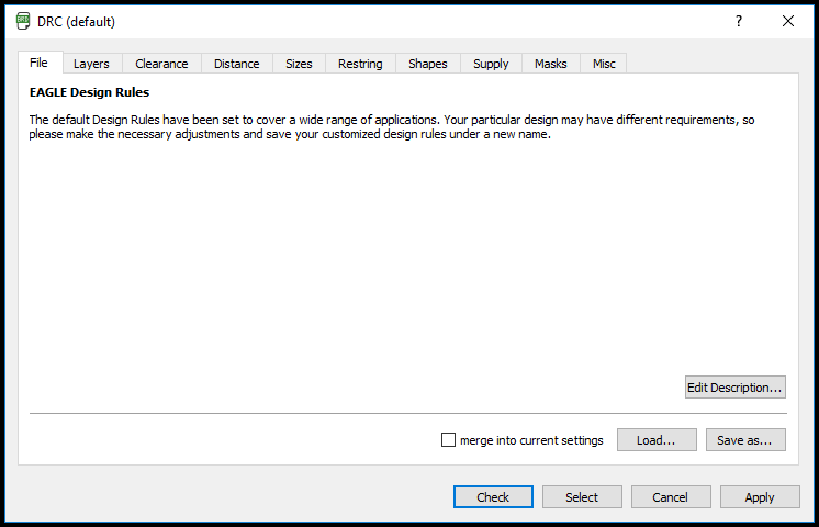
Designing a PCB in Autodesk EAGLE is a fun and rewarding process, but it doesn’t happen in isolation. While you might be designing your board in your PCB design software, at the end of the day, you’ll likely ship off your files to a manufacturer to create a physical circuit board. And in the world of PCB manufacturing, there are some very real physical constraints that you need to pay attention. This is where a Design Rule Check comes into play.
Rather than designing your board without a care for your manufacturer’s limitations, a Design Rule Check allows you to establish a set of boundaries for trace widths, component spacing, via diameters, etc. It’s only after you have all of these rules set up that you can then go about completing your design process, knowing that any issue with these manufacturing-specific constraints will be flagged in Autodesk EAGLE when you run your DRC.
In the example design, we’ve been working on we left our design rules at their default. But as you dive into more professional projects you’ll likely set up some custom design rules before you ever place a component or lay down a track. Until that time arrives, let’s walk through how to run a basic Design Rule Check on our project.
- Open your PCB layout (.brd) file from your Autodesk EAGLE Control Panel.
- Select the DRC
 tool on the left-hand side of your interface to open the DRC Setup dialog.
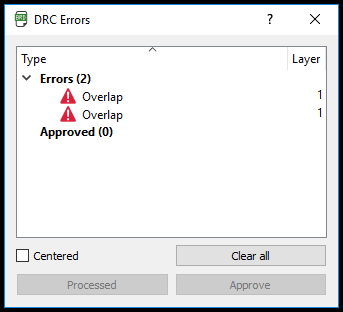
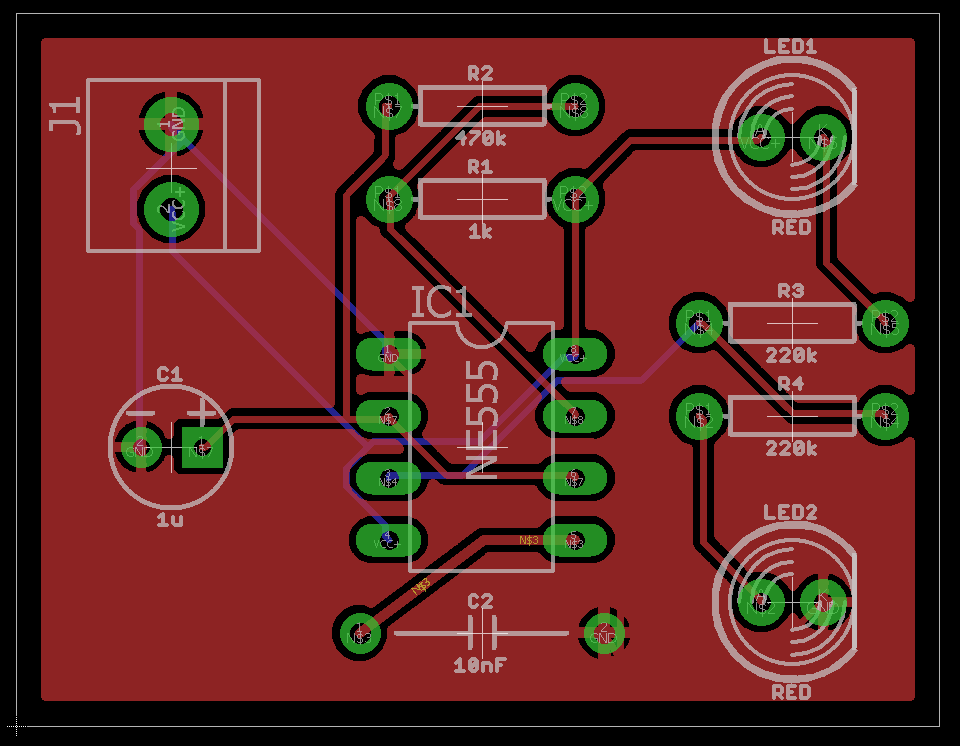
When we ran the DRC on our completed LED flasher project we didn’t have any errors, so we decided to intentionally make one by overlapping a trace with a component pad. When we ran our DRC check again, we had two errors for overlapping objects on layer 1, which is our top layer.
By selecting this error, you can see that we have a white box on our PCB layout that shows us exactly where the issue is located. Coupled with an error description, this becomes a detective-like process of figuring out what needs to be adjusted.
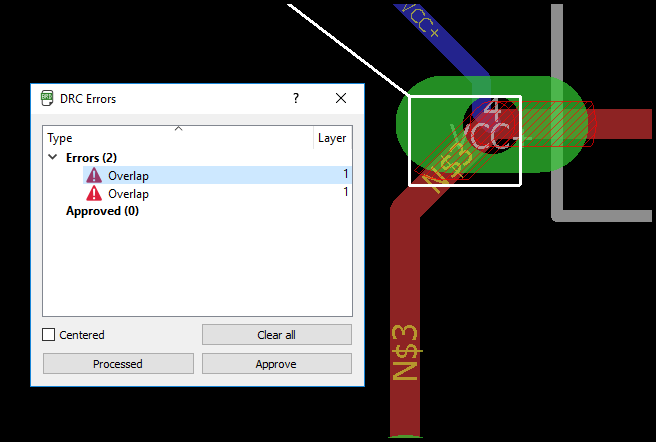
In our example, we’ll go ahead and rip up the overlapping trace and route it again, so it isn’t run across a pad. Once that’s complete, we can run our DRC check again, and we’ll get a DRC: No error message. Success!
Adding a Copper Pour to Your Layout
There are many reasons to add copper pours to our design. Adding a copper pour to your board adds a great finishing touch that gives your board a professional look while also providing a common layer for all of your ground and power signals. Shielding or heat dissipation.
And while we might be adding this copper pour last, you can also add it at the start of your layout process. This will make routing complex boards that much easier when you have a common connection point for all of your ground signals. To add a copper pour, do this:
- Select the Polygon
 tool on the left-hand side of your interface.
 - At the top of your interface, select your top layer (1 Top) in the Layer Selection dropdown, and then enter an Isolate setting of 0.012” to provide enough clearance between your ground signals and copper pour.
- Now left-click at the bottom-left origin point of your PCB outline and begin drawing a red line along each edge of your board.
- When you return to your origin point left-click again to finalize your polygon outline. Your solid red polygon should now turn into a dashed one.
Once your setup is complete, all you need to do is select the Ratsnest ![]() tool on the left-hand side of your interface, and you should now have a red copper pour before your eyes! Go ahead and repeat this process for your bottom layer, this time for Layer 16 instead of Layer 1.
tool on the left-hand side of your interface, and you should now have a red copper pour before your eyes! Go ahead and repeat this process for your bottom layer, this time for Layer 16 instead of Layer 1.
Adding Silkscreen to Your Layout
The final touch of polish to add to your design is silkscreen text and drawings. This part is entirely optional and doesn’t really add any functionality to your design. What it does do though is add some great context and aesthetics to an otherwise bland looking circuit board.
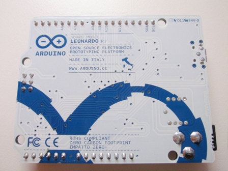
For example, if you were to try to use an Arduino Uno without any of the silkscreen to identify the pin numbers for the digital and analog signals it would be a huge pain. But with silkscreen identifying those pins is easy. When in doubt document; we always recommend adding a layer of silkscreen text as the final finishing touch to your design. Here’s how to do it:
- There are several tools you can use to add silkscreen, including the Wire
 , Text
  , Circle
  , Arc
, Arc  , Rectangle
  , or Polygon tool. Choose one on the left-hand side of your interface.
 - Now you need to choose which layer to draw your silkscreen on. Select either 21 tPlace (top silkscreen layer) or 22 bPlace (bottom silkscreen layer) from your Layer Selection dropdown.
- Lastly, left-click on your PCB layout to start drawing or adding silkscreen text.
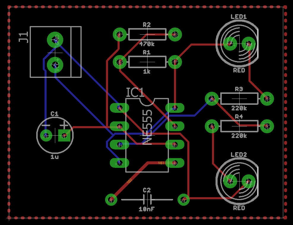
We kept things simple with a silkscreen name for our LED Flasher in the bottom-left corner of our layout, but don’t hold back! Get creative and draw/write whatever you want.
You Are Now Ready for Manufacturing
It’s official; your layout is officially complete! The PCB design process requires a ton of work, from learning how to place your components to skillfully completing your routing and finally diving into some detective work with a Design Rule Check.
As your designs get more advanced and complex, you can expect to spend hours on your PCB layout process, and for a good reason. At this stage of your journey, you’re tasked with translating what was once a two-dimensional representation of a circuit on a schematic into something that is going to be physically manufactured. That’s a huge responsibility!
At this point, it’s time to save your project, sit back, and admire all of your hard work. If you haven’t already gotten in touch with your manufacturer, now would be the time to do so to get a quote for your design and see what kind of files they might need to make their magic happen. If you do not have a manufacturer picked out, OSH Park is a great place to start. Stay tuned for our future PCB Manufacturing Basics Series where we’ll be covering how to make all the files you need to send to your manufacturer in Autodesk EAGLE.
Making your first PCB layout in the free version of Autodesk EAGLE is just the tip of the iceberg! Get the full experience today by subscribing to Autodesk EAGLE.