PCB Manufacturing Basics Part 3: DFM & Reviewing Your Design Files
This is it, the moment you’ve been waiting for, it’s time to get your PCB manufactured! Many beginner engineers think the whole design process ends when they route that final net on their board layout. But as we’ve shown in our Manufacturing Basics Series, there’s a whole world of post-design processes that need to be completed to get your board in shape for production. In Part 1 of this series, we showed you how to create Gerber and NC Drill files which your manufacturer uses to create a bare board. And in Part 2 we showed you how to create a Bill of Materials (BOM) in Autodesk EAGLE so you can source all the parts you’ll need for assembly. In this final stage of your manufacturing prep, it’s time to give your design files a final stamp of approval.
The Review Process at a Glance
By examining your design files before sending anything off to your manufacturer, you’ll ensure that you won’t hit any issues down the road. After all, who wants to deal with back-and-forth emails and phone calls from their manufacturer? We’ll be breaking this review process down into three steps:
- Step 1 – Validating Your Gerbers. Any seasoned designer can tell you that the Gerber format is far from perfect, which means you’ll need to check each file closely for errors. In this step, you’ll look at your Gerbers and design files side-by-side to catch any potential mistakes.
- Step 2 – Checking for DFM Issues. In this step, you’ll be looking for things like whether you have any silkscreen text on a pad or any open loops. Everything we cover here relates directly to whether you have any issues that will affect the manufacturability of your design.
- Step 3 – Sending Your Files. This is the final milestone and involves packing up all of your design files into a ZIP package and sending it to your manufacturer. But rather than relying on email to complete this process, we’ll be looking at some alternatives.
Step 1 – Validating Your Gerbers
Here’s the deal, Gerbers are a timeworn file format, dating back over 30 years. By all standards, this is a primitive file format that is still an industry standard. Bit crazy, right? Its widespread use could be attributed to its start as the only file format for photoplotter machines that manufactured PCB designs back in the day. Or maybe Gerbers get the job done good enough, and there isn’t enough pain to bring about some needed change.
Despite their widespread use, Gerbers are far from perfect and have known issues when translating designs into physical bits of data. Ask any engineer this, and you’ll hear a variety of stories, like Gerbers completely jumbling a layer stackup, or fab houses not being able to understand provided Gerber extensions and sending them back to the engineer to correct at the last minute. Or even worse not getting the proper copper coverage due to resolution issues. Point being, Gerbers have some real limitations that beginner designers need to understand, like:
- Juggling Separate Files
Today’s Gerber files will always need to generate a separate physical file for each layer of a PCB. For you, this means keeping track of a handful of files and their extensions and also validating each one visually on every single design you complete. - No Layer Stack Definitions
While each file in a Gerber represents a layer of your design, the Gerbers themselves do not communicate how this layer stackup is organized. You’ll still have to manually communicate to your manufacturer how all of your Gerber files fit together. - No Electrical Connectivity Information
Gerbers don’t include any information about how your nets are supposed to be connected, it’s just shapes defining copper data. If you need your bare board tested during manufacturing, then you’ll need to include a separate netlist file. - No Drill Data
Gerbers also don’t include any information about the size and placement of drill holes on your board. For this information, you’ll be relying on yet another file called an NC Drill File. Sometimes this NC Drill file is generated on a different scale than your Gerbers, which can muck things up a bit if you aren’t paying attention when creating it. - No Part Information
You’ll also need yet another file to define exactly which parts need to be sourced and assembled on your bare board with a Bill of Materials (BOM). Any issues between your BOM and Gerber can hold up your manufacturing process, causing some unpleasant delays that you, or your boss, won’t be happy. - Geber Resolution issues
The current Gerber standard (RS-274-X) can yield a resolution of 0.01 mils (0.00001 Inches). Now I know what you are thinking, “That is tiny!”. However, when you route smaller traces with tightly rounded corners, you will start reaching these limitations quickly. Your polygons and small copper areas will be manufactured with gaps.
We think we’ve driven our point home well enough – Gerbers are an extremely limited file format. But at the same time, they’re also an industry standard and will continue to be so in the future. While newer file formats are trying to capture the attention of the PCB manufacturing industry, none of them have had a lasting impact as Gerbers have. So they’re here to stay, and you’ll just need to accept their limitations by doing your due diligence and check the quality of their work.
To do this, you’ll want to go about visually validating that your Gerber files line up exactly with the design that you made in Autodesk EAGLE. We can use the Gerber Viewer in Circuits.io to do this, here’s how:
- Open your PCB layout (.brd) file in the Autodesk EAGLE Control Panel.
- Select the Make
 button at the top of your interface to open the Eagle: Autodesk Export to Manufacturing dialog.
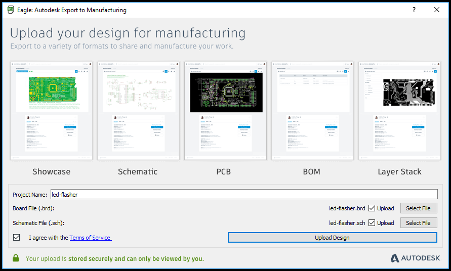
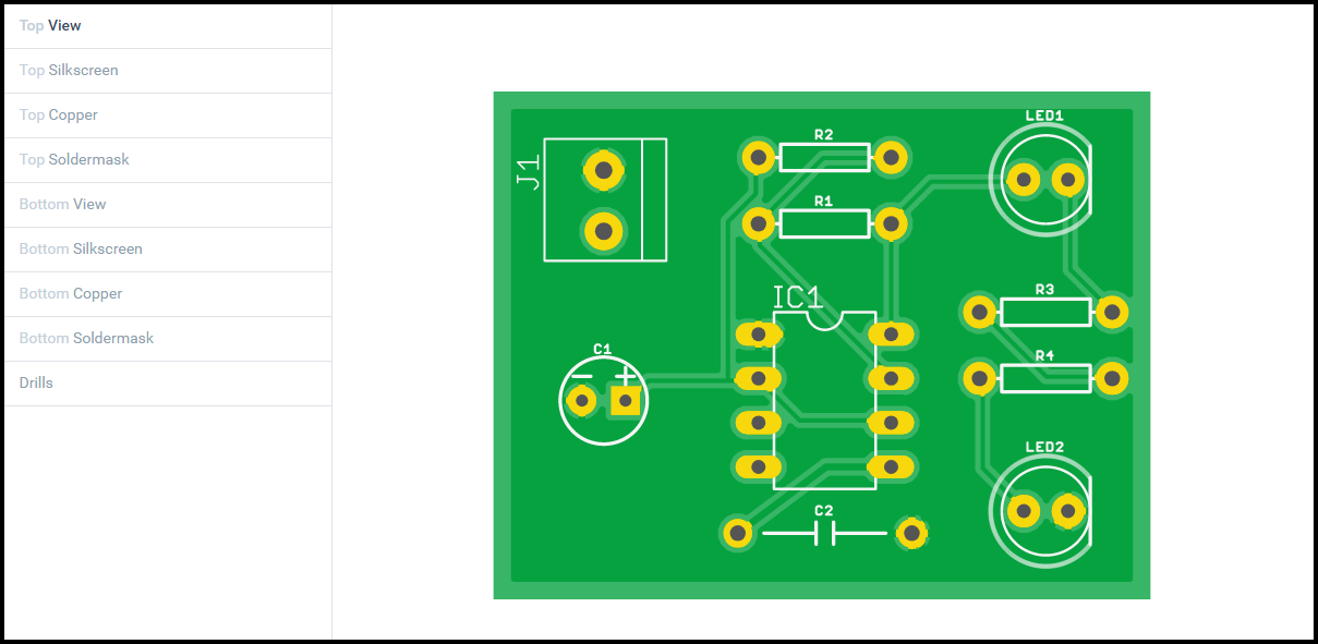
Now that you’ve got your Gerber files open in Circuits.io, you can begin to compare each layer side-by-side with those in Autodesk EAGLE. Back in your PCB design tool, you can start filtering by the same layers you’re looking at it in Circuits.io to get a visual comparison. Here’s how:
- Open your PCB layout in Autodesk EAGLE and then select the Layer Settings
 tool on the left-hand side of your interface.
 - In the Display dialog, choose the None button to turn off all your layers. Next, left-click the layers you want to see that will match what you’re looking at in Circuits.io. For example, if you want to cross reference your silkscreen you’ll select Layers 21 tPlace and 25 tNames.
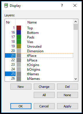
When you have matching layers in both Circuits.io and Autodesk EAGLE, go ahead and compare both. Does your silkscreen match? Do your copper patterns match? How about your soldermask? If you see a difference, then make a change in Autodesk EAGLE to correct it, and upload your design to Circuits.io to compare again.

If you’re not too fond of uploading your design to Circuits.io and would prefer to view your Gerber files in a local desktop application, then you can use a Gerber Viewer. There’s a ton of free and paid versions out there. Here are a few to try for Windows, Mac, and Linux:
- Windows – Viewplot Gerber Viewer
- Mac – MCN Gerber Viewer
- Linux – Gerbv Gerber Viewer
Whichever Gerber Viewer you choose to install, the process of comparing between your Viewer and Autodesk EAGLE will be the same. You can follow the instructions we laid out in PCB Manufacturing Basics Part 1 to generate a local copy of your Gerbers to open in your viewer.
Step 2 – Checking for Design for Manufacturing (DFM) Issues
After visually validating all of your Gerber files, it’s time to move on to some final Design for Manufacturing (DFM) checks. What is DFM? It’s basically a methodology of designing a PCB that makes it as manufacturable as possible. Because while you can have the most beautiful design in the world, if isn’t practical to physically create, then you’ve wasted your time.
The tricky part with checking for DFM issues is that each manufacturer might have a different set of standards based on the machinery and processes they use. However, there are some general DFM guidelines that you’ll want to look for that will apply to any manufacturing process, including:
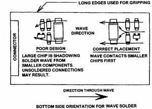
Component Orientation
Did you orient all of your components of a similar type in the same direction? This is going to help ensure that all of your parts get soldered evenly when ran through a soldering oven. If you’ve got your parts in a bunch of different orientations, then it’s likely you’ll get a board back with unsoldered connections and shorts.
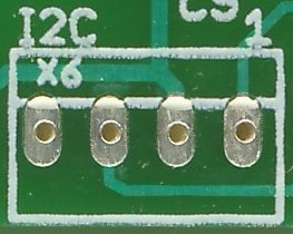
Silkscreen On Pads
Did you check to make sure that you don’t have any silkscreen on your pads? Those pads are exposed copper, and placing silkscreen text on them will make soldering your components tough. Be sure to look for any overlaps when checking your Gerber files.
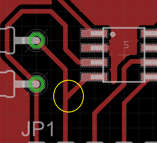
Open Loops
Did you check to make sure that you don’t have any open loops on your board layout? This is a common mistake that can occur after doing a post-routing cleanup as you make edits to existing traces. By connecting a new net but not removing the older one, you’ll create an endless loop.
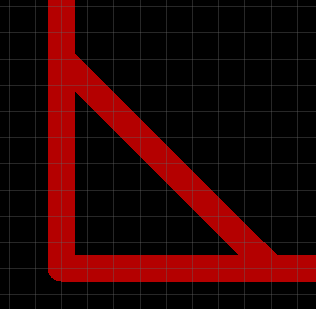
Acid Traps
Did you check to make sure you don’t have any acute traces that are angled less than 90 degrees on your layout? Acute angled traces have a chance of trapping chemical residue when your board is being cleaned, resulting in your traces delaminating from your board later. While this isn’t as big of an issue today, be sure to check with your manufacturer to see if they have trace angle guidelines.
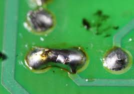
Solder Bridges
Did you check to make sure that your pads have enough clearance from your soldermask? If not then you might wind up with two solder joints forming an unintended connection. To prevent this from happening, double-check that you’re using the right pad dimensions per your component’s datasheet and that you have enough clearance between your pads and soldermask layer.
Design for Manufacturing (DFM) is like an entire world of knowledge on its own, and these five tips are by no means an exhaustive list of everything to check for on your design. Luckily, most manufacturers these days offer a free DFM check. A great example is Advanced Circuits, who offers a FreeDFM™ File Check that scans all of your design data for manufacturability issues.
Step 3 – Sending Your Files to a Manufacturer
At this point, you’ve done the due diligence to visually validate your Gerbers and check for any manufacturability issues you might have missed. If you have any issues during steps 1 and 2, then you’ll want to correct them in Autodesk EAGLE and re-generate all of your manufacturing documentation. When you’re ready to move ahead, then it’s time to send your design files off to your manufacturer. But first, let’s talk about email.
In the past, sending design files to a manufacturer was usually handled through email. This might have made sense back in the day when managing an inbox didn’t feel like a second job. Today though, we’d never recommend this practice. Why? Imagine having to keep track of potential revisions and updates to your manufacturing files in an endless email thread, multiplied by dozens or even hundreds of designs. It’s a recipe for disaster. These days most manufacturers will have a direct upload method for all of your design files. You’ll want to upload everything in a tidy zip package, which needs to include at the bare minimum:
- Your Gerber files that will describe the copper patterns for each layer in your PCB design.
- Your NC Drill file which will define the location and size of every drill hole on your PCB layout.
- A readme.txt file that lists every filename you’re including, a brief description of what each file is, and your contact information.
This list is the bare basics, and we would highly recommend checking with your manufacturer to see if they require any additional documentation. If your manufacturer does both bare board fabrication and part assembly, then you’ll also likely need to send them your Bill of Materials (BOM).As an alternative to directly uploading your design files, you might also consider using a storage system like Google Drive or Dropbox to store and share your design files. These services will allow you to provide your manufacturer with a direct download link, and they can choose exactly which files they want to download. This also offers the benefit of being able to keep your design files organized and accessible in the same place for both yourself and your manufacturer.
As an alternative to directly uploading your design files, you might also consider using a storage system like Google Drive or Dropbox to store and share your design files. These services will allow you to provide your manufacturer with a direct download link, and they can choose exactly which files they want to download. This also offers the benefit of being able to keep your design files organized and accessible in the same place for both yourself and your manufacturer.
Wait for the Magic to Happen
After sending your design files to your manufacturer, it’s time to sit back, relax, and wait for the magic to happen. Depending on the complexity of your design and which manufacturer you choose you should expect to receive a board back in a few days to a few weeks. If you’re lucky, you won’t be getting a call or email from your manufacturer after you first contact them to make your board. But if you do, then prepare to put on your detective hat as there’s likely an issue with some of the data in your manufacturing files. If you’re still on the fence about which manufacturer might be the best fit for your design, then take a look at these three options:
- OSH Park – A great option for keeping costs low, OSH takes designs from a bunch of engineers, sticks them on one panel, and saves everyone money along the way. Their delivery timeframe is 12 days for a 2 layer board.
- Advanced Circuits – One of the biggest and well-known fab houses around in the US, these guys offer a 1-5 day delivery on boards with 1-10 layers.
- Euro Circuits – For those over the pond in Europe, Euro Circuits is another highly rated fab house that delivers within 2-7 days for 1-16 layer boards.
Once you get your board back in the mail from your manufacturer, then it’s time to celebrate! We started this journey all the way back in our Schematic Basics Series, and here we are today, with a completed physical circuit board in hand. Something is amazing about being able to design, and then see it come to life before your eyes through a physical manufacturing process. This is the magic of electronics design, where you can transform your ideas into reality.
Ready to start designing and manufacturing more complex designs? Upgrade now to an Autodesk EAGLE Subscription.