Antenna design and RF layout are the two most essential components of any wireless system. You can take two identical RF products, each with a different antenna design and layout and get two vastly different RF performance ranges. What’s the difference? It’s all about quality and consideration taken during the design process.
The folks over at Cypress have assembled a significant application note that that covers the breadth of Antenna Design and RF Layout guidelines. These two subjects deserve books of their own and years of practice to master fully. But to get started, this Everyday App Note will arm you with all of the fundamental knowledge to make your next wireless systems project a success. Here’s a sampling of the design guidelines that you’ll find inside.
For Antenna Design
A Meandered Inverted F-Antenna, or MIFA, needs to be length-adjusted to account for antenna radiation impedance and frequency. The tip and length of a MIFA antenna are determined by the thickness of your PCB as shown below:
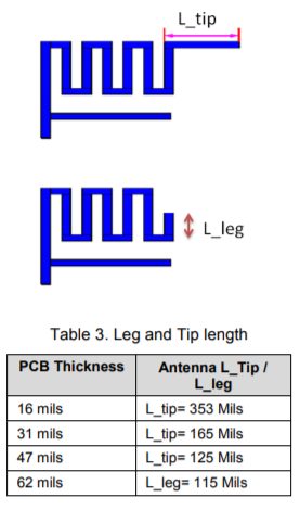
Since it’s easier to cut antenna length than adjust it, it’s always recommended to start with a full -length antenna. Then based on PCB thickness you can use the length cutting method to tune your antenna quickly.
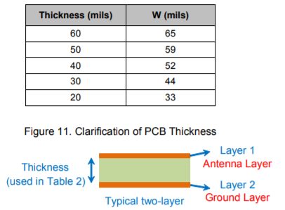
The thickness of the top and bottom layers of a two-layer PCB will also determine your antenna feed consideration. In this setup, the top layer contains the antenna, and the bottom layer serves as an RF ground plane. The table below shows a guideline for how thick your insulating layer between the top and bottom layers needs to be:
For RF Layout
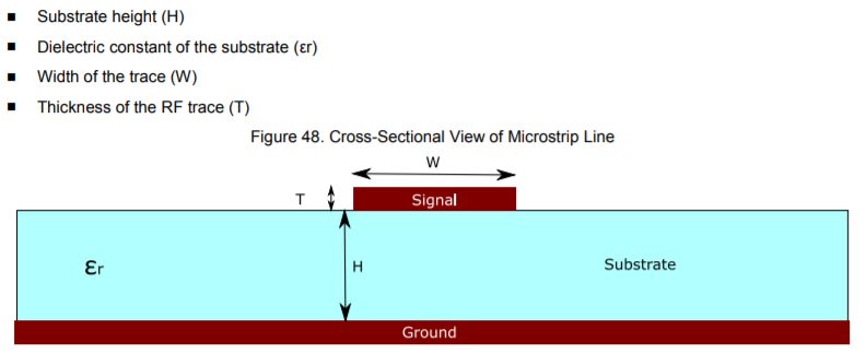
There are two popular transmission line types that will effectively transmit an RF signal from source to load and ground, Microstrip and CPWG. The microstrip line runs a signal on the top layer of a board, with the return path on the bottom substrate. These transmission lines are easy to construct, simulate, and fabricate. When designing a microstrip line, you’ll want to pay attention to the following factors that affect impedance:
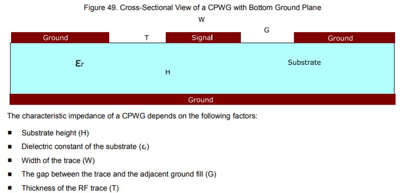
A CPWG transmission line is similar to a microstrip but includes a copper ground filling on both sides of the trace. These transmission line types typically provide better isolation and EMI performance for RF traces. They also have a lower loss at high frequencies when compared to microstrip lines. Factors that affect impedance for a CPWG transmission line include:
Download It Now
Above was just a small sampling of all the antenna design and RF layout guidelines you’ll find in today’s Everyday App Note from Cypress. Inside you’ll learn about both the fundamentals and best practices for:
- Antenna design, including antenna parameters, types, and guidelines for placement, enclosures, and ground planes.
- RF layout, including impedance matching, RF transmission lines, and ground plane considerations.
- Antenna selection, including how to take advantage of low-cost solutions from Cypress for use in Bluetooth Low Energy (BLE) applications.
Don’t cut your range short, download the Antenna Design and RF Layout Guidelines App Note now!