Everyday App Note: How to Successfully Design a Mixed-Signal PCB With Partitioning
Today’s Everyday App Note comes from Henry W. Ott, one of the leading experts on electromagnetic compatibility (EMC). One of the most significant misconceptions about mixed-signal PCB design is the effectiveness of using a split ground plane to isolate analog and digital ground signals. Henry thinks there’s a better way and discusses it in this app note.

Who Is This App Note For?
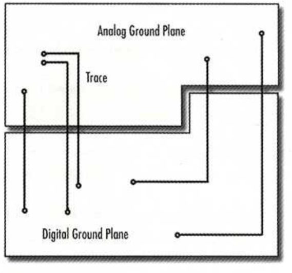
Are you struggling to prevent digital ground currents from interfering with low-level analog currents on your mixed-signal PCB? If so, this app note is for you. These sophisticated designs typically require isolation of analog and digital ground planes, but this presents a problem. What happens when you route signal traces across a split in the ground plane? Hello, radiation and crosstalk. This app note discusses an alternative strategy using partitioning to keep those analog and digital ground signals separated.
Why Should You Read This App Note?
Many designers only consider where their current signal flows but not the path taken by the return current. The basic principles of electromagnetic compatibility (EMC) show what’s wrong with this mindset:
Current should always be returned to its source as efficiently as possible through the smallest loop area. By splitting a ground plane into analog/digital sections and then routing signals over the split, you create a larger return current loop than desired.
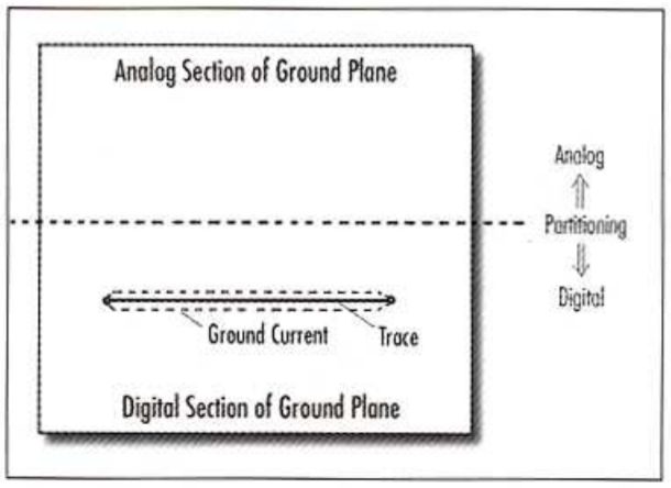
So what’s the solution? Rather than splitting your ground plane, Henry Ott recommends adopting a partitioning strategy. With this strategy, you’ll have only one ground plane, and your PCB layout is split into separate digital and analog sections. Analog signals only get routed in the analog section. Digital signals only get routed in the digital section.
Partitioning is just the start of the process though. You can have a perfectly partitioned PCB layout but still unintendedly route digital logic traces in an analog section, which will lead to EMC issues. Because of this, Henry discusses the following three-step strategy:
- Partition your PCB with separate analog and digital sections.
- Route digital and analog signals only in their respective sections.
- Place analog to digital converters on the split between both sections.
If your layout is done properly with this strategy, then your digital ground current won’t interfere with your analog ground current. Sounds like an ideal world!
Ready to get started with partitioning for your mixed-signal PCB layout? You’ll need to hone your routing discipline and component placement to make it work. Download this application note now to learn more!