Designing PCBs for the FCC: A Guide for Every Electronics Designer
You’ve got the best idea in town for an electronic product, but are certifications halting your success? According to studies by Intertek, you aren’t alone. Nearly 50% of all first-time electromagnetic compatibility (EMC) tests result in failures. We all know what that means – respins, skyrocketing costs, and the potential demise of your product. In this blog, we’ll be taking the mystery out of FCC certification so you can design electronic products that pass the first time, every time.
The FCC and Electronics Design
The Federal Communications Commission (FCC) was founded in 1934 and acts as a gatekeeper for the radio spectrum. It knows what devices are being used and on what frequencies all over the United States. Why do devices need to be regulated in the first place? To help safeguard against potential interference. The FCC keeps things in check by ensuring that every product meets specific limitations for RF emissions and electromagnetic compatibility.
Are you a hobbyist? If so you can stop reading here. The FCC lets a hobbyist make five devices from a single design without requiring any testing. Per section 15.23 of 47 CFR Ch.1:
“(a) Equipment authorization is not required for devices that are not marketed, are not constructed from a kit, and are built in quantities of five or less for personal use. (b) It is recognized that the individual builder of home-built equipment may not possess the means to perform the measurements for determining compliance with the regulations. In this case, the builder is expected to employ good engineering practices to meet the specified technical standards to the greatest extent practicable.”
For startups and professional designers, read on to learn more about FCC compliance for your upcoming electronics project.
What Does the FCC Test?
The FCC requires that electronic devices marketed and sold in the United States meet specific guidelines for electromagnetic compatibility (EMC) and radio-frequency (RF) emissions. The two general test categories are:
- EMC Testing. This test will measure the strength of the EMF field that your device generates under a variety of operating conditions.
- RF Testing. This test will measure the generated EMF fields within specific radio frequencies on the electromagnetic spectrum.
Based on these two test categories, one might assume that you only need to be concerned with the FCC if your device has an RF component. Not so fast. Any electronic device with a clock speed above 8 KHz is going to produce some type of interference or noise. The FCC goes on to define how devices radiate their interference, either intentionally or unintentionally.
Intentional Radiators
These devices intentionally emit an RF signal and include all typical wireless modules like WiFi, Bluetooth, Zigbee, etc. These devices have to be tested and certified by the FCC before they can be sold and marketed in the United States.

Unintentional Radiators
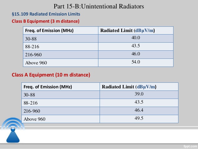
These devices unintentionally emit interference/noise and can include things like switching noise from a power supply, extended clock traces, or antennas created from a sloppy ground pour or a trace stub. While these devices do need to be tested the results don’t need to be sent to the FCC.
Whether your device is an international or unintentional radiator, you’ll need FCC documentation to support it. This can come in three flavors:
- Verification. Devices are verified through testing at either an independent or FCC-verified testing lab. The reports for verification need to be kept on file with your product should the FCC come knocking.
- Declaration of Conformity. These devices are tested at an accredited FCC testing lab. The test reports will also need to be kept on file with your product but don’t need to be sent to the FCC.
- Certification. Devices requiring certification are tested at an accredited FCC testing lab. The test reports will be sent to the FCC to be reviewed, filed, and hopefully passed.
FCC Costs and Fines
The testing and certification process for FCC compliance can be costly. The first step to understand your expected investment is to identify whether your device is an unintentional or intentional radiator. Once defined, you then need to decide whether your device requires Verification, Declaration of Conformity, or Certification paperwork. For unintentional radiators, Subpart B of Section 15.101 for 47 CFR 15 lists the following device types and their required compliance:
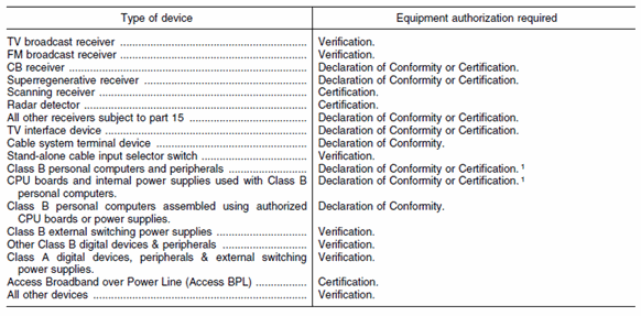
The intentional radiator will require Certification with few exceptions. The testing and certification process for these devices can take anywhere from four to six weeks. We’ve also seen testing centers that took ten months to work on a device. Mileage will vary depending on your product specifications and the responsiveness of your chosen testing lab.
For costs, you’re looking at anywhere between $8,000 and $20,000 to have a device Certified. Devices that just need Verification or a Declaration of Conformity run between $1,000 and $2,000.
There’s also the sore subject of non-compliance fees. On July 1, 2016, the FCC raised the fines for products found in violation of its rules. The maximum penalty has risen from $37,500 to $47,350 for each violation of a product or each day that a violation continues to persist. Continuing violations have also risen from $400,000 to $473,402.
Point being, messing around with FCC violations is serious business and can mean the difference between your product’s success and failure. You can read more about increased FCC fines here.
The Path of Least Resistance for FCC Compliance
If all this information is sounding overwhelming, we have a solution. There’s a type of certification that the FCC offers called Modular Certification. This basically allows you, as the designer, to purchase wireless modules that are already certified which can be used in your design.
This is an excellent approach if you want to avoid all of the details, costs, and paperwork associated with FCC emission testing early on in your product’s development. There are a ton of companies that make modules for BLE, WiFi, Zigbee, GSM, and other wireless technologies.
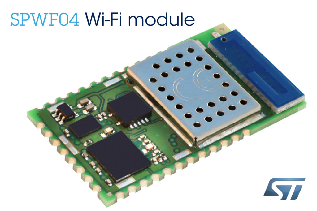
They all go through the same painstaking process of FCC approval and sell modules that include a chip, balun, antenna, crystal, and shield that can be quickly soldered onto a PCB. When you use one of these certified modules, you won’t have to worry about FCC intentional radiation testing at all.
We typically see design teams using these modules when they’re planning to produce a low volume product. This allows them to get quickly started with their development process without tying up valuable resources with FCC busywork. Once the product takes off, and the financials are in place then a team often looks into designing their own RF technologies. There are two types of modules to know about:
Pre-Certified Modules
These modules are produced by a manufacturer that has taken all of the steps needed to obtain FCC certification. By using these modules, you’ll get the benefit of FCC compliance, but you’ll also be restricted in your choice of antennas.
The OEM that produces these modules will work with an EMC testing lab to certify a handful of antennas that will work with the transmitter. This means that as the end user, you’ll need to choose an identical antenna that was used to pass FCC guidelines. Most pre-certified modules will come with an integration manual that outlines how the device can fit into your existing design project.
When considering a pre-certified module, keep the following in mind:
|
Positives |
Negatives |
|
|
Non-Certified Modules
Maybe you don’t have the budget to spend on certified modules, or you’ll be making your own RF device sooner rather than later. If so, then non-certified modules are worth a look. These modules haven’t gone through official certification testing, meaning you’ll need to do the testing yourself. However, they do offer a cost-effective way to prototype ideas quickly.
Disclaimer: This road is not for the weary. We’ve seen enough companies integrate a non-certified module into their board only to fail at the testing lab. Thousands of dollars later and weeks delayed getting to market taught them a tough lesson. Only use a non-certified module as a temporary measure, not an in-field solution!
When considering a non-certified module, keep the following in mind:
|
Positives |
Negatives |
|
|
Subassemblies & Exempted Products
If you’re still looking for ways to avoid the hassle of testing your product, you have two final options we’d like to mention. First, there are several exempted product categories that your device can fall into. These categories can be found in the Code of Federal Regulations, Title 47, Part 15, Section 15.103.
There’s also the option of keeping your device within the FCC’s definition of a subassembly. These are defined as sub-systems of digital devices that are not marketed as part of a larger system. If they are marketed as part of a system, then they’ll need to comply with FCC regulations. You can read all about the details about subassemblies in Section 15.101e of Title 47.
The Path of Mastery for FCC Compliance
So you’ve decided to design your own RF module and handle the testing of your device. You’ve got a long road ahead of you, but the experience will be worth it. While we can’t cover the full RF design process in this blog, we’d like to guide those on the path of FCC mastery with some helpful tips:
Leverage Your Testing Center
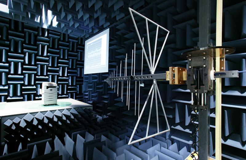
FCC-accredited testing labs will be your most significant resource when working towards FCC compliance. They’ll be your go-to expertise to determine requirements and testing needs based on your product specifications. When you make contact with a testing lab be prepared to sign an NDA, disclose all of the specifications of your product, and explain how you plan to sell and market it. The best place to find an FCC-accredited testing lab is from the FCC’s Test Firm Search page.
Thoroughly Research Your Components
We’ve seen our fair share of designers work with component vendors that don’t certify their modules. This is a great cost-cutting strategy during the prototyping phase. However, when you leave that module in for your FCC testing process, don’t be surprised when it comes back failed.
To avoid this mess we recommend doing thorough research on all of your components. In an ideal world, we’d say to use only pre-certified modules, but you need to consider all of your components, not just the wireless ones. Here are some tips to keep in mind:
- Always check to make sure you aren’t using components that can cause interference issues with the rest of your device. Sensors with long traces are one of many examples.
- Pay careful attention to wires and cables that connect to external components. These will always emit electromagnetic (EM) radiation.
- For pre-certified modules, double and triple check that you’re using antennas that were used in the original certification. If you don’t then you’ll need to submit for testing yourself.
Identify Unintentional Radiators
Have you seen ferrite beads on a power cable recently? These little cylinders are a sign of last-minute solutions to an emissions disaster. It’s also an indicator that the designer either didn’t have the time or didn’t spend the time worrying about the noise their device was creating.
Instead of waiting for disaster to strike, know upfront that EMI problems tend to have many sources for their problems. You can sometimes get away with toning down the loudest EMI sources to get through testing, but your best bet is to reduce all of your radiators are their various frequencies.
To do this, you first need to identify all of the unintentional radiators in your design. This can include things like:
- Digital clocks
- Switching power supplies
- Motor drivers
- Components with repetitive current pumping
All of these devices will be seen on an emissions test, and your goal is to recognize what those noisemakers are, and how to tone them down before beginning your EMC test.
Plan Your Circuit Strategy
After identifying all unintentional radiators, you can then begin the process of reducing their power consumption or limiting their higher harmonic outputs. Keep the following guidelines in mind when planning your circuit strategy:
- If your signal is being used in a low-bandwidth path, you don’t need immaculate square waves and picosecond rise times. For I/O drivers this means that it just needs to be powerful enough with ninth harmonic content and above.
- DC motors can be an EMF disaster. When designing DC motors that use armature brushes, you’ll likely need to include a 100 pf or 0.1 uF capacitor at the motor for proper arcing. You’ll also need two common-mode chokes between the PCB and motor and a flyback diode or snubber circuit on the motor to protect the driver transistor.

Reduce Your Onboard Antenna Size
Antennas come with their own source of emission problems which usually stem from a collection of smaller antennas. Because of this we recommend always reducing your onboard antenna sizes if possible and keeping them enclosed between ground planes. You can also use onboard layers and flooded ground planes around signal lines to help reduce EMI and improve signal integrity.
Be Mindful of External Connections
Wires connecting your PCB to an external connection are one of the most common sources of radiation due to their length. Be sure to use twisted-pair wires to create a tight common-mode characteristic between two wires. This will help to produce a ground referenced signal and maintain integrity and impedance in your external wire connections. It will also help to avoid creating a loop antenna from an open loop of wire.
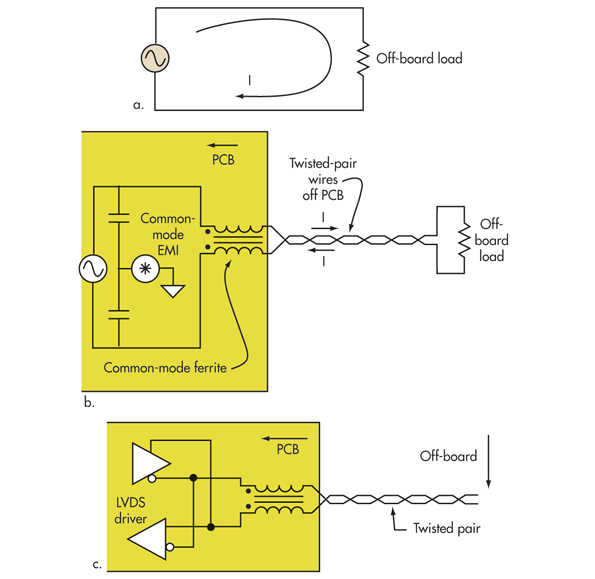
Keep in mind that twisted-pair wires will not help reduce common-mode radiation from both wires since they radiate the same signal. In this instance, you’ll need common-mode chokes to reduce radiation.
For high-speed wires like USB and Ethernet use common-mode chokes inserted at each end of the twisted-pair wires. This will ensure that common-mode EMI from the PCB doesn’t make it into the wires. It also attenuates any ground bounce between your device at both ends of the wire.
For power connections, be sure to fit both wires through the same common-mode ferrite choke. Doing this will cancel out DC currents and minimize magnetic fields created in the ferrite. The choke should be built onto the PCB at the exit of the enclosure.
Consider a Shielding Box
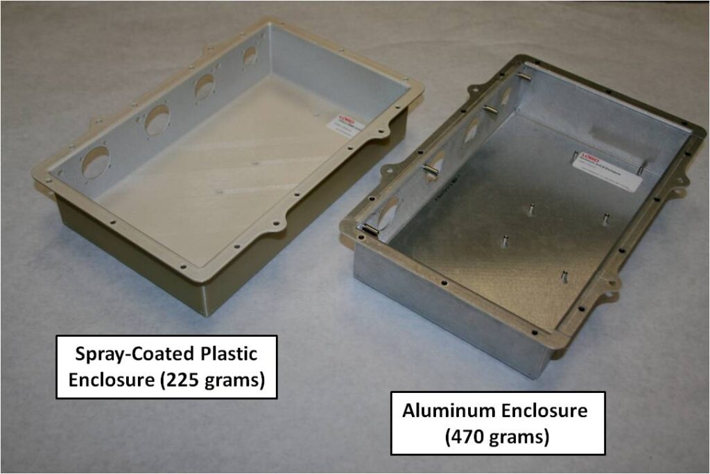
Consider adding a shielding box for designs with a variety of noise sources. If you’re working on a consumer device in a plastic case, then you can opt for a conductive coating inside the case. When working with your mechanical team on the enclosure be sure to define requirements for your Faraday cage early on in the design process.
PCB Layout Strategies
There are a ton of layout strategies that can impact emissions in an RF design. We can’t cover them all here, but here are a few guidelines to get you started:
Reduce Trace Lengths
Always keep your trace lengths as short as possible as this will help to reduce EMI issues. How short? That depends on your design. As a general guideline keep your signal input to receive path as short as possible. Also, keep receivers, and their inputs close together. These two placement considerations will naturally lead to shorter traces.
Mind Your Grounding Practices
Ideally, use one solid ground plane in your design with carefully routed return paths. Using two separate ground planes results in different references for sections of your circuit and increases the chance for interference.
Also be sure to connect any bypass or decoupling capacitors directly to ground to reduce any chances for interference. A path to ground that is too long will increase the risk for EMI.
Use Bypass Capacitors to Reduce Noise
You can place bypass capacitors near DC components to reduce noise and create a cleaner DC signal. For placement, you can use the bottom side of your board, which provides extra space for vias and fanout traces on your top layer.
Are You Down With the FCC?
Certifications like the FCC don’t need to halt the success of your next great electronics product. When in doubt, always opt for using pre-certified modules to get your design running quickly. These modules provide an easy and effective path for FCC compliance without any of the busywork. For those daring to design their own RF modules, be sure to rely on your most valuable resource, your testing center, along with the design strategies we covered here.
Ready to design your first FCC-approved electronics device? Try Autodesk EAGLE for free today!