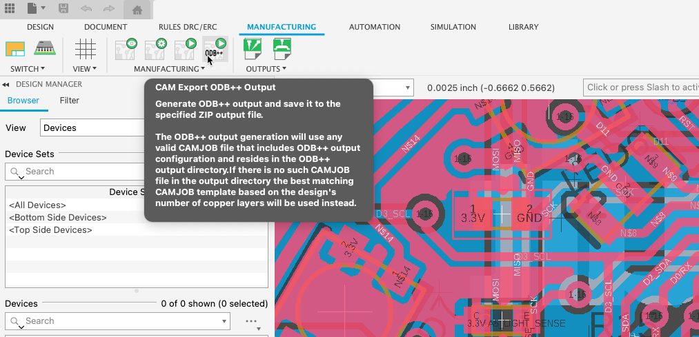
Here’s everything you need to know about ODB++ export, a highly requested feature from our community that’s now available in Fusion 360.
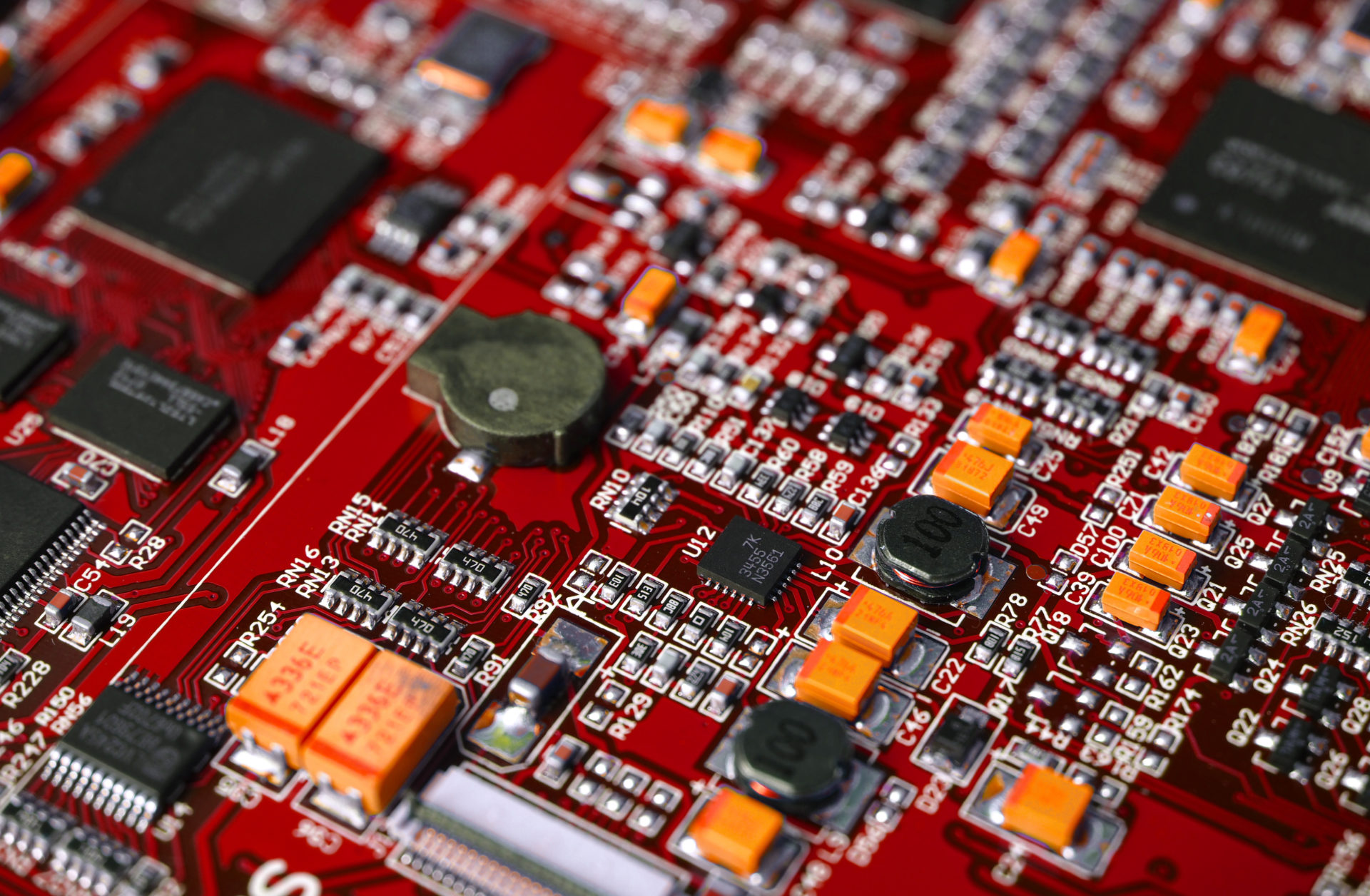
Have you ever dismantled any electronic device, toy, or gadget? If the answer is a yes, you must have seen a circuit board consisting of many components. From tiny gadgets to bulky appliances, these circuit boards are to be found everywhere. In electronics jargon, these boards are referred to as PCBs or printed circuit boards.
If you haven’t ever seen a printed circuit board, don’t worry. Here’s an image of a PCB:
What’s the purpose of PCBs?
Now that we know that PCBs are an essential part of all electronic devices, the question arises, “Why is this so, and what purpose do these boards serve?.” The answer is simple. PCBs provide mechanical support for the electronic components and interconnect them electrically.
PCB production starts with a blank PCB sheet made from fiberglass or some other non-conductive material laminated with copper layers. These copper layers are etched to realize the board design. PCB production is a complex process with multiple process steps. Major steps in PCB fabrication include CAD design, design printing, copper removal, component placement, and soldering.
After the excess copper is removed from the board, the PCB design looks like as shown in the image below.
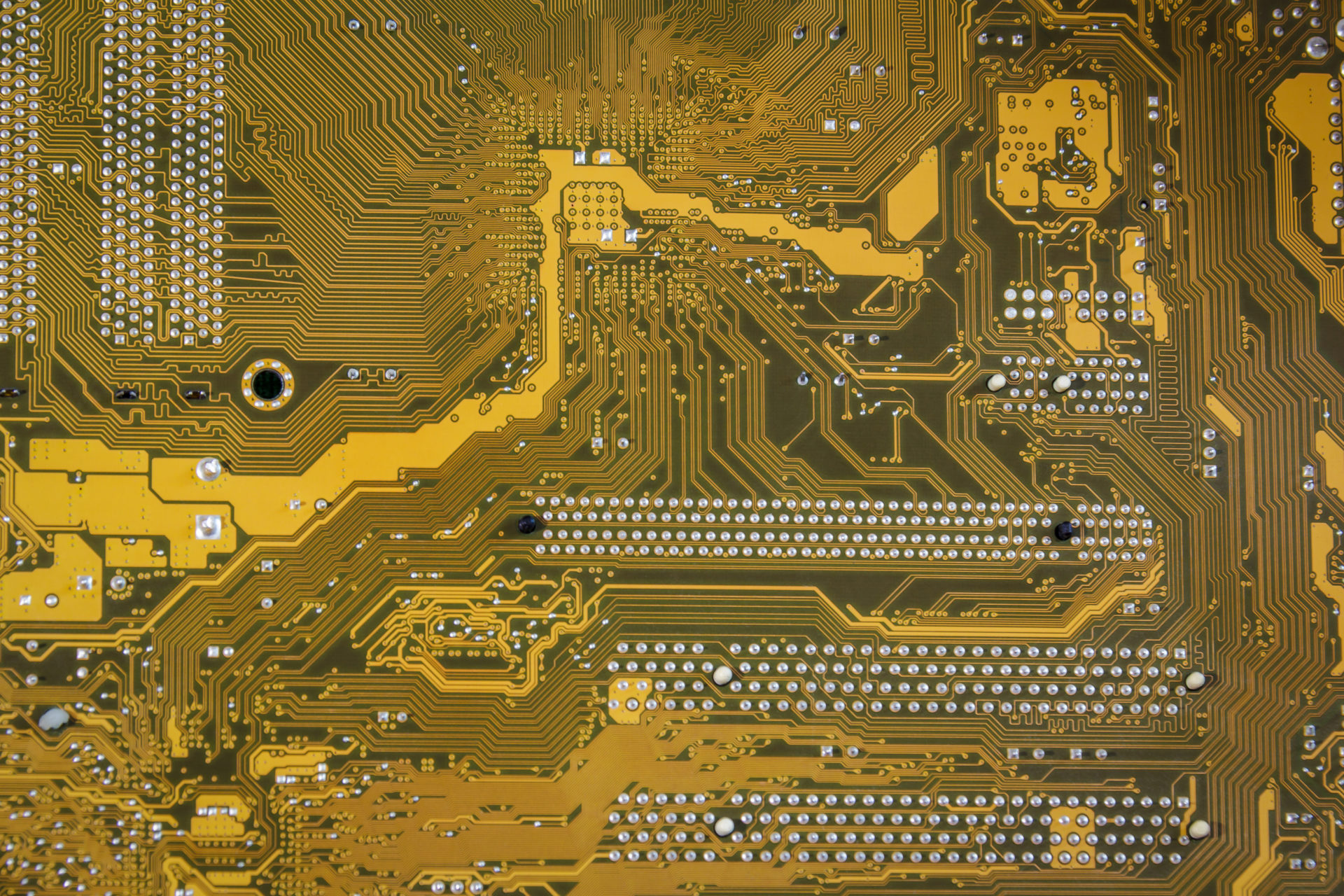
The copper traces or pathways on the PCB interconnect electronic components. After the etching of copper traces, components are placed on the PCB and are soldered. In terms of component placement, PCBs are of two types: through-hole and SMT (surface mount technology). A vast majority of modern PCBs are assembled using robots, and automated machines make use of SMT technology.
Importance of CAD and CAM in PCB production
PCB production starts with PCB designing. PCB designs are created using specialized software packages known as CAD (computer-aided design). The primary objective of CAD software is to create a virtual representation of a physical object.
CAD software like Fusion 360 allows engineers to design, test, and debug circuit board layouts without creating a physical prototype. Therefore, the use of CAD software not only saves time but also cuts down development costs. Some powerful features of CAD software include auto-routing, design reuse, data management, and 3D visualization.
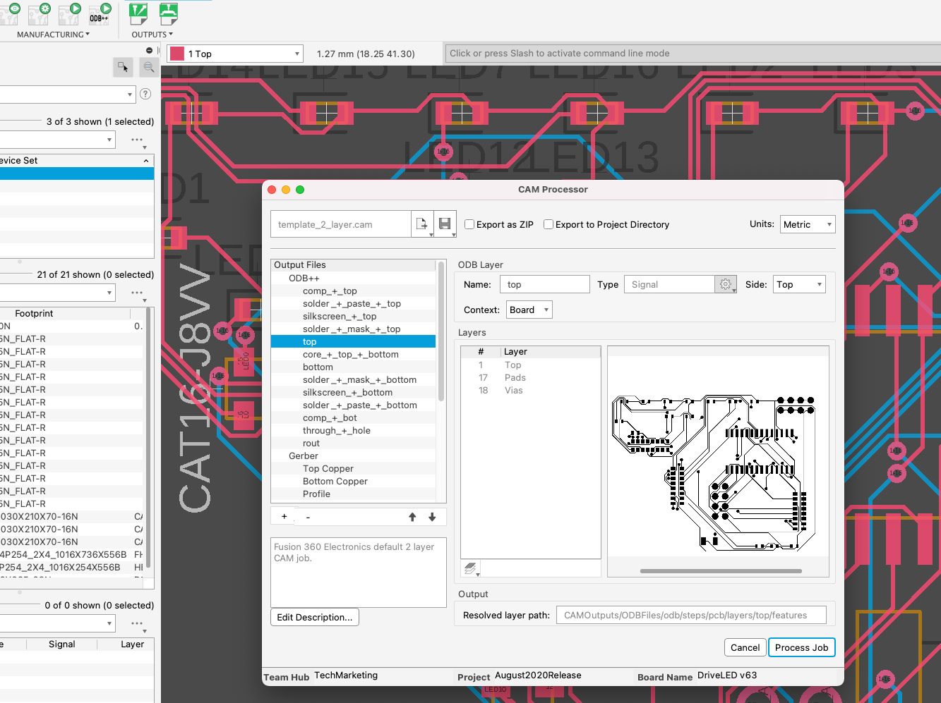
After completing and verifying the CAD design, it’s passed on to the CAM (computer-aided manufacturing) processor. The purpose of the CAM processor is to realize the virtual CAD design into a physical product. As different companies often design the CAD and CAM systems, a uniform data exchange protocol is absent. To solve this problem, several CAD-CAM data exchange protocols have been developed. These protocols serve as a bridge between incompatible CAD and CAM systems. Examples of PCB CAD-CAM data exchange protocols include ODB++ and Gerber.
What is ODB++?
ODB++ is a CAD-CAM data exchange format developed by Valor Computerized Systems in 1995. This data format aims to exchange information between design and manufacturing facilities within a PCB fabrication unit. ODB++ is the leading data exchange format in the PCB manufacturing industry, and therefore all major PCB design software packages support this data format, now including Fusion 360.
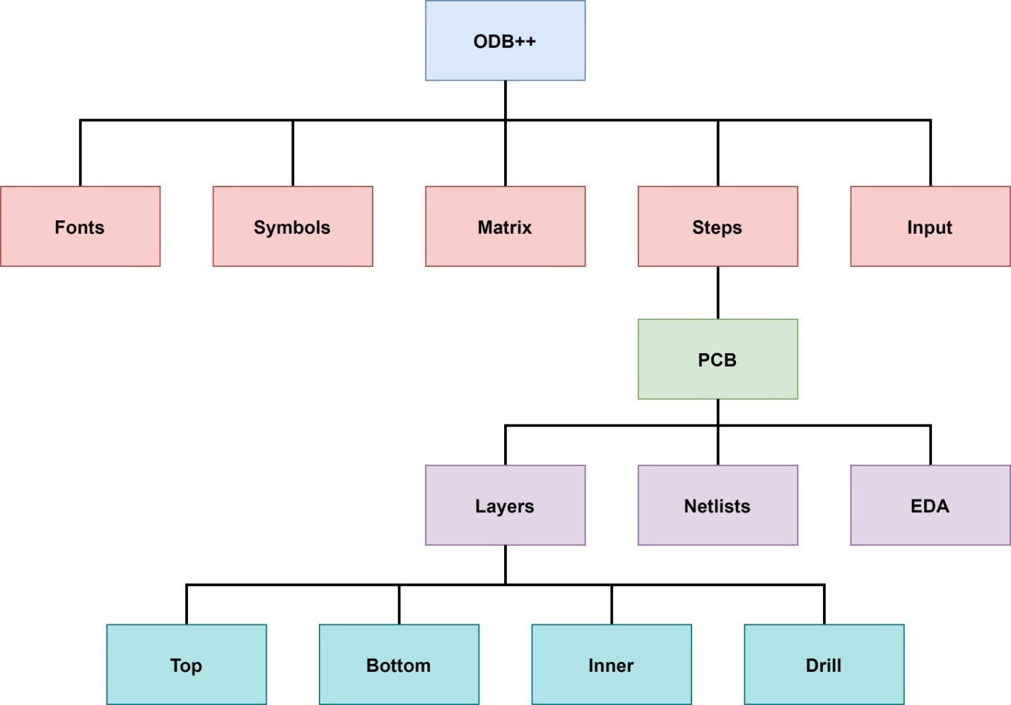
ODB++ File Structure
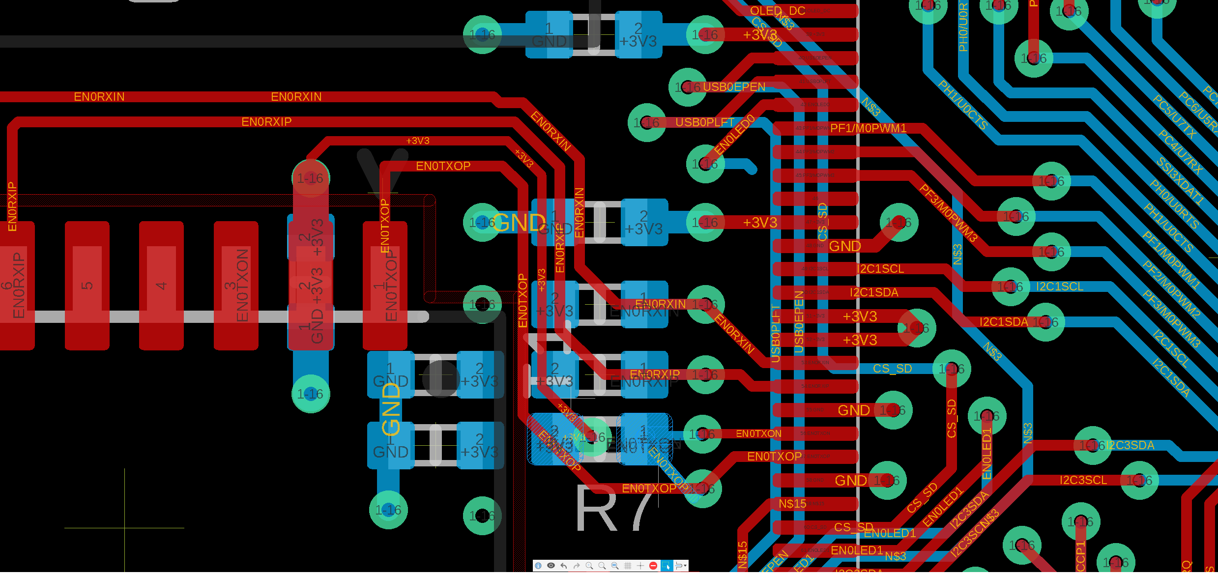
ODB++ format uses a standard file system structure consisting of a hierarchy of files and folders. For data transmission, however, a single compressed file is generated by Fusion 360. Due to the hierarchical structure of this data format, very detailed information can be included, such as conductor layout, drill data, fabrication data, dimension data, bill of materials, and component placement data. Take a look at this illustration of ODB++ file structure for a full breakdown:
One great feature of ODB++ is that all the files are ASCII-readable. Hence, advanced users can directly read the database files without using any special extraction program. Many old legacy systems use binary database files which cannot be read without a special format conversion program.
In the past, most vendors preferred binary databases due to limited computer storage. However, the capacity of hard disks has increased dramatically in the last two decades. In addition to that, the emergence of efficient compression techniques has allowed the vendors to opt for ASCII databases. In ODB++ format, larger data files are stored in standard UNIX compress format.
Benefits of ODB++
ODB++ offers multiple advantages to PCB designers, fabricators, and manufacturers, some of which are listed as follows:
- All the design data for manufacturing, assembly, and testing is packed in a single file.
- ODB++ supports integrated DFM at all layers.
- Minimization of supply chain risks due to minimal data transmission errors.
- Increased automation at all steps of circuit board designing and manufacturing.
- ODB++ is supported by all major vendors of CAD, CAM, and DFM tools.
- ODB++ features a complete layer table consisting of the layer name, layer type, and order of layers.
- As opposed to Gerber format, the difference between pad and conductor is clear.
Comparison of Gerber and ODB++
Gerber and ODB++ are the top data exchange formats in the PCB manufacturing community. Gerber is the most widely used data format in PCB manufacturing and is often regarded as industry-standard. However, Gerber faces strong competition from ODB++ due to its superior performance and accuracy. Despite holding 90% of the market share, Gerber format has some serious limitations. First, Gerber format does not include layer stack-up information which can lead to inaccurate ordering of copper layers. Secondly, Gerber format does not include drilling information, increasing the risk of missed-out holes.
As opposed to Gerber, ODB++ format eliminates the need for multiple CAD and CAM files by providing a single hierarchical data structure. ODB++ includes layout and drill information and incorporates details regarding BOM, dimensions, testing, and fabrication. This comprehensive information significantly reduces the risk of human and machine-induced errors. Due to enhanced accuracy, speed, and turn-over time, ODB++ is a superior data format compared to Gerber. ODB++ export is a highly requested feature by our community, adn we’re excited to now offer it in Fusion 360.