This blog will guide you through the basics of getting started with Fusion electronics, offer practical tips, and help you become more confident using the software.
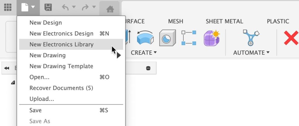
When you are first getting started with Fusion Electronics, it’s easy to feel overwhelmed by all of the features and tools at your fingertips. I get it—it’s a powerful software, and it can seem like there’s a lot to learn. But trust me, once you get familiar with the basics, you’ll see how intuitive and integrated the workflow is. In this blog, I’ll guide you through getting started, share a few practical tips, and help you feel more comfortable navigating the essentials. Whether you’re new to ECAD software or just transitioning to Fusion from a different E-CAD platform, you’ll be designing more confidently in no time.
From the Fusion Preferences it will only take a few clicks to have Fusion always launch directly to the electronics workspace.
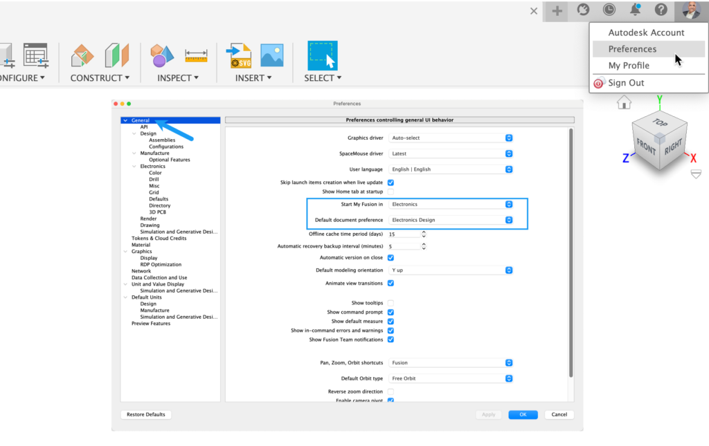
The next time you launch Fusion, it will automatically begin in the Electronics Document workspace.
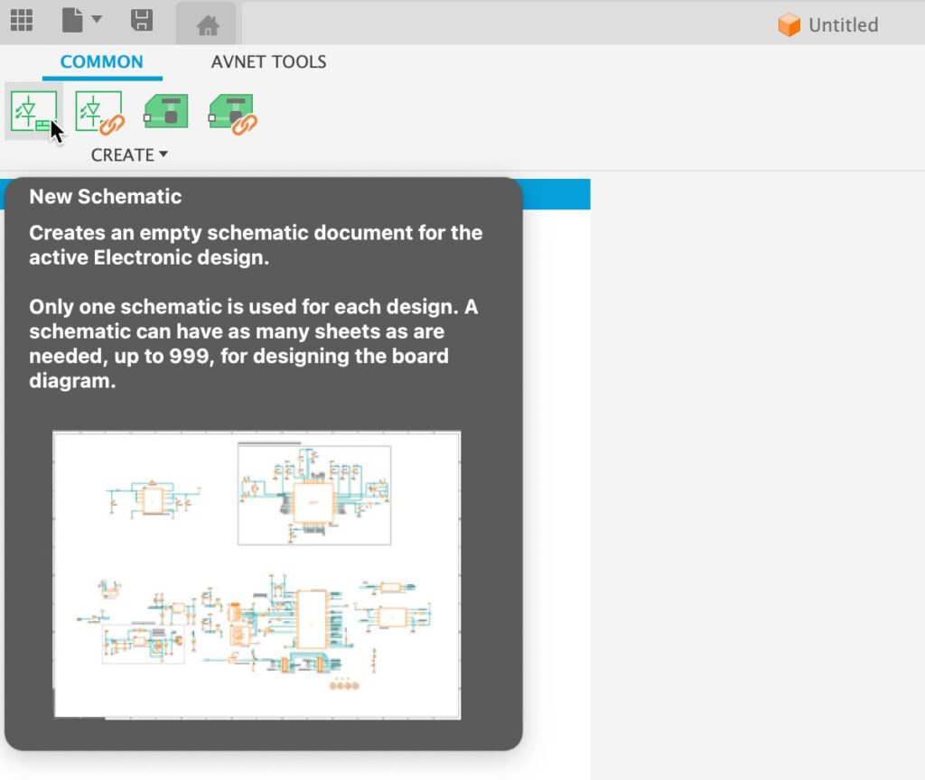
The initial screen will appear once the Fusion Electronics workspace is the Electronic Document. This is the system by which Fusion will always keep the PCB and the Schematic synchronized. If you have an existing Schematic and Board, you can link them using the link icons. If the schematic and PCB are not synchronized, you will be alerted and provided insight into the possibility of fixing it using the synchronizer. For our example, I will be invoking a new Schematic.
Fusion electronics schematic editor
This action will open the Fusion Schematic Editor. If you are an EAGLE user, you will notice many similarities, which shouldn’t be surprising considering that Fusion Electronics is based on Autodesk EAGLE. The top toolbar has icons for the most commonly used commands, which go from left to right. Under each icon command, there is a list of related commands.
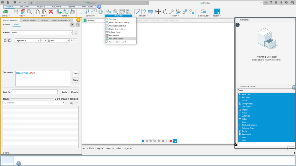
Many things are going on here, but I plan to unpack it in the simplest way possible.
- This is going to be referenced as our Menu Toolbar. Here, you will access additional commands and options while editing your Schematic.
- It is our first set of panels. These panels are fully customizable. They can be re-ordered or tabbed based on your preference. You can also move them about the workspace. The Design Manager is one of the most valuable panels since it allows me to navigate our design easily.
- This is another set of panels for our Inspector and Selection Filter. After selecting assets on the Schematic, the properties that can be changed will appear in the inspector panel.
- It is the panel of our schematic sheets.
- The selection Filter helps you filter precisely which assets you want to select in the workspace. Very useful for large designs.
Adding components to schematic
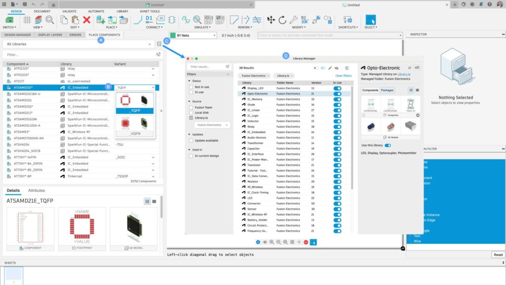
One of the first actions taken in the Schematic is adding parts to our Schematic. To access the available parts in Fusion Electronic, select the Place Components Panel (A). The list of components that appear is based on the libraries that are currently in use. Notice that I have nearly 33k components available at this time. Selecting a component in panel (B) will provide a preview of the component and its attributes at the bottom of the screen. If the part has more than one footprint assigned to the schematic symbol, you can easily select the drop arrow and activate the footprint you need. To add a part to the Schematic, left-click and hold, then drag the part to the Schematic workspace.
Access the Library Manager (C) to browse more of our available libraries. The library manager (D) gives you access to your Fusion Team and Managed libraries. If you have been using EAGLE Managed libraries, you will also see them here. Make sure to select Library.io and browse the available options. Selecting any library from the manage library dialog will provide you with a preview of the content of the selected library.
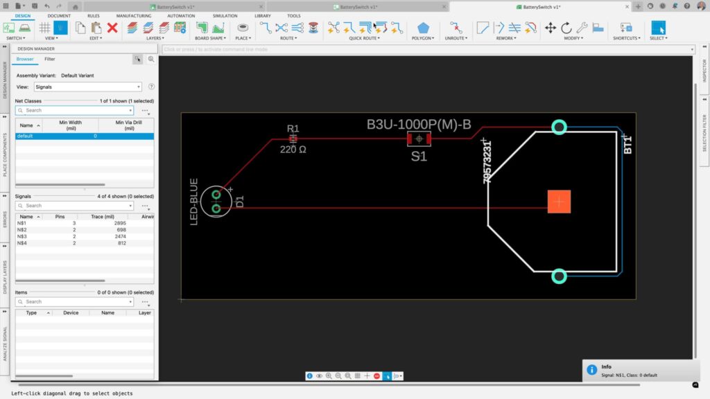
Defining connections in the schematic editor
| BOM | |
| Library Name | Component |
| Battery Holder | 79573231 |
| Switch | 1000P |
| Resitor | Chip-0402 |
| Opto-Electronic | LED_Radial |
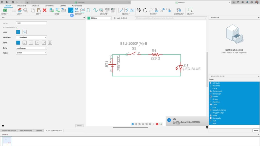
For our example, I’ll keep it simple and place a few components on our schematic workspace. I used the Frames library to get a frame. I switched to the Battery library to find a battery holder, and I found the resistor I wanted to use in the Resistor library. In the Opto-Electronics library, I found the LED and finally grabbed a switch from the switch library.
We will be using the NET (A) command to define our connection. I strongly advise you to keep working on the default .1-inch grid for the Schema ic. This will avoid unconnected assets in the Schematic. While running your NET, notice a bubble appears when the connecting point has been reached.
Take a look at the following video tutorial on how to design your first schematic:
Defining shortcuts in Fusion electronics
Before we move on to the board, I’d would like to show you how to define shortcuts that way we can optimize your design time. Fusion provides an excellent, straightforward way to define single-key shortcuts. Many are already pre-defined in the electronics workspace.
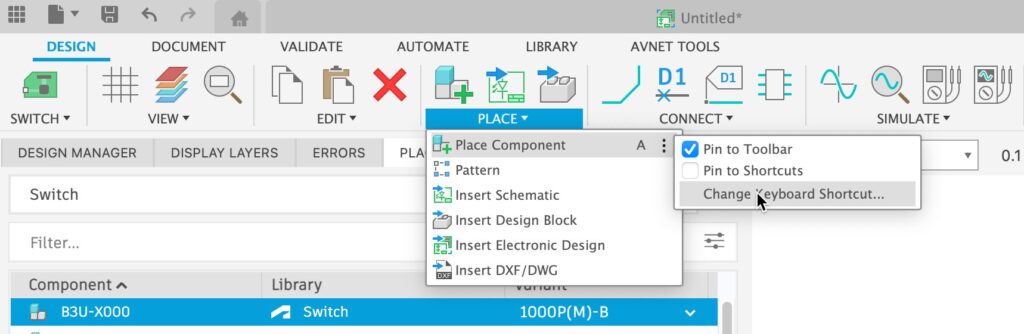
Notice that pressing ‘A’ will automatically invoke the Place Component dialog box. It is possible to change these default assignments by clicking on the three dots on the right side of the command and selecting the “Change Keyboard shortcut”. You can also use key combinations (Modifiers) for shortcuts such as Shift, Control, Alt/Option, and Command with an alphanumeric key.
The electronics workspace does offer one more shortcut option, which is included in Autodesk EAGLE. This second option allows you to assign shortcuts to a command string. This shortcut option needs to use a modifier, so assigning a command string to a single keystroke action is not possible.
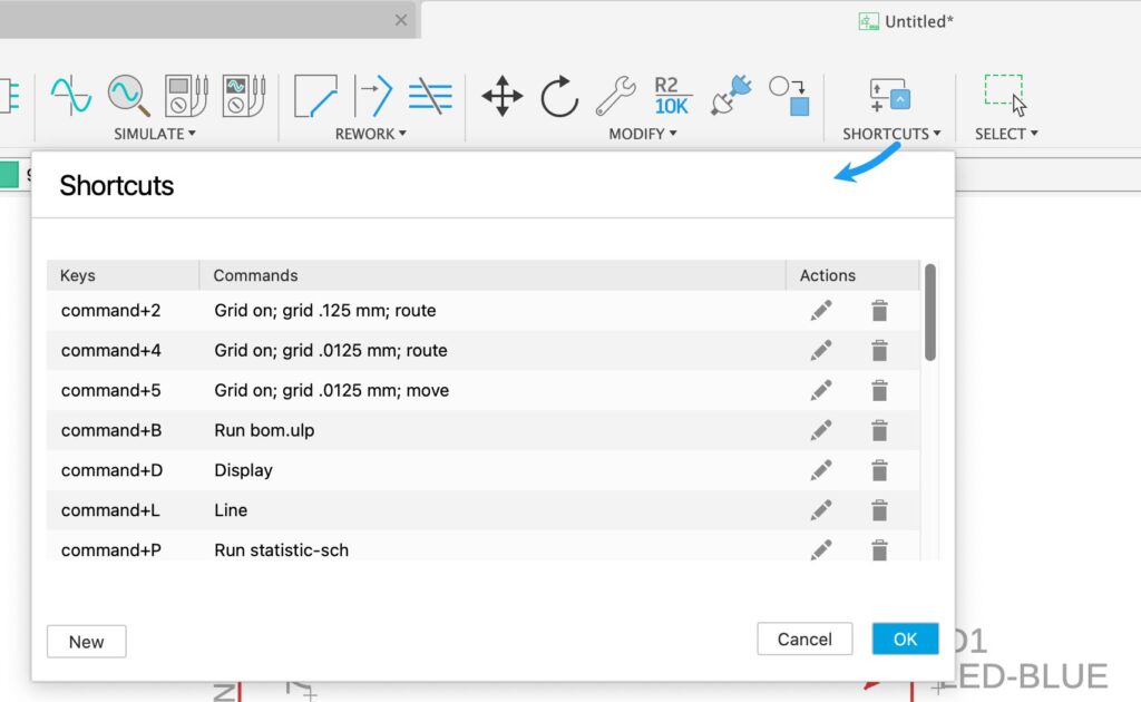
Here is one I defined to invoke the schematic BOM easily. Press and hold Command + B, invoking the Bill of Material for this Schematic. Another example is changing the grid size and visible status to enable the manual route command. CMD+2 “Grid On; Grid .125 mm; route). Creating new shortcuts is easy. Select New and follow the dialog. When creating a new shortcut, you will be warned if there are conflicts with existing shortcuts.
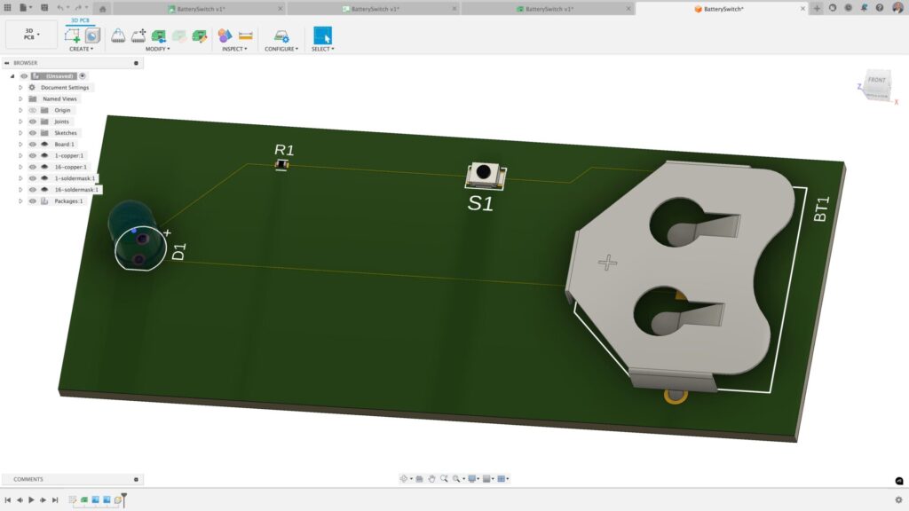
Moving to the PCB
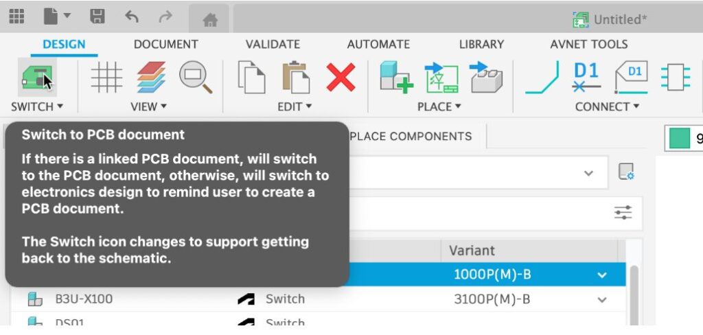
Moving from Schematic to PCB is as easy as selecting the “Switch to PCB Document” icon. This action will open the PCB editor and populate the PCB with the footprints from the Schematic, and the resulting connections will be in the form of signals or airwires.
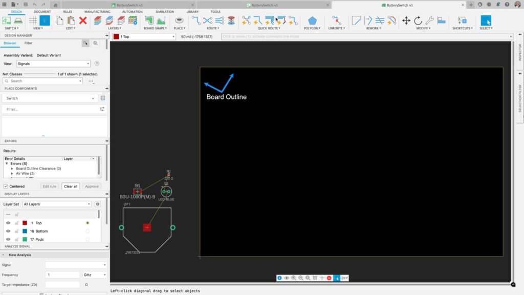
The default board size appears on the PCB. You can click and hold the outline to resize it. Before you start moving your component onto the board, I strongly recommend that you set your design rules and preferences; if you have a prototype or manufacturer in mind, find out the Constraints they wish to follow. Doing this early will save lots of time and resources. It may even save you from spinning up prototype boards.
Design rules and preferences
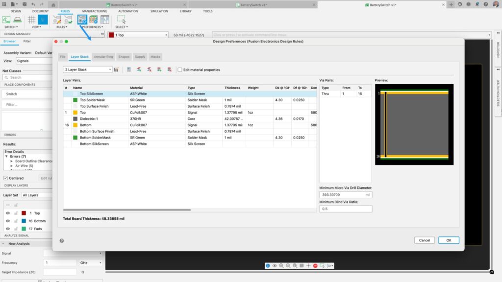
Design Preference is where you will establish the global constraints for your PCB, such as layer stack, layer materials properties, Annular Rings, supply, and mask properties. You will find access to the Design Rule preferences in the Rules Tab. Many PCB manufacturers already have rules established in EAGLE format. You can load these DRC parameters from the Rules Tab. You can access the Design Preference dialog. Make sure you are making changes that accommodate this design success.
Besides changing your layer stackup to accommodate your design, there isn’t much else I recommend changing here. The default values should work great for the vast majority of designs.
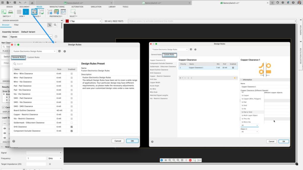
Design Rules provide the option between General Rules and Custom Rules. General Rules are the default values assigned to the design constraints. These default values should be able to satisfy any manufacturer. You should also know that the General Rules constrain the Autorouter.
Custom rules allow you much more flexibility regarding assigning constraints since they empower you to establish rules between specific signals or between signals and components, polygons, Design Classes, and more. To learn more about Design / Rules Custom rules, please checkout this blog. Custom rules, including Quick Route, will be considered when doing manual and interactive routing.
Populating the PCB in Fusion electronics
With the constraint rules established, now is an excellent time to begin adding parts to our PCB. As you move the cursor around your PCB, you’ll notice that assets are highlighted. The highlight established the asset boundary by which it is selectable. Left-click and hold to select the component and place it in the PCB workspace. Notice how the Signal automatically extends and contracts as the component is moved.
Use the Route command to route your signals and the center mouse button to change layers if necessary. When switching layers, Vias (points of transition) will automatically appear.
Design your first PCB in Fusion by following along with this video tutorial:
Creating manufacturing files in Fusion electronics
To get the PCB prototype or manufactured, you will need to export PCB manufacturing files, which Fusion Electronic supports the most common formats, ODB++ and Gerber files. Please review the blog I recently published to learn how to export your PCB for manufacturing, please review the blog I recently published.
This is a basic introduction to the Autodesk Fusion electronics workspace. I may have used the most straightforward example dataset, but I wanted to demonstrate the basic steps to get you up and running as soon as possible on your next innovation. Soon, I will cover much more of the department design capabilities in Fusion. With what you learned today, why not download and start your 30-day trial today and get your next innovation started?