PCB Manufacturing Basics Part 1: How to Generate Your Gerber and Drill Files
There’s no greater reward than spending hours designing every last detail of your PCB and then finally getting your board back from your manufacturer. The wait can seem like an eternity when you first hand-off your design files, but when you receive that package on your doorstep, it’s like an engineer’s Christmas! In our PCB Basics Series we’ve gone through the entire design process, starting with a visual representation of your circuit in schematic design, and then moving on to squeezing all of that theory into a physical footprint with components and traces. Now it’s time to move on over to the post-design process to get ready for PCB manufacturing.
It’s at this juncture where you’re tasked with assembling all of the files and documentation that your manufacturer will need to successfully produce your board. And once they have everything they need, you get to sit back and wait for a package to arrive. But how does a manufacturer know how to make your PCB? They can’t use your native EAGLE files. You’ll have to send them Gerber Files and Excellon Drill Files.
Gerbers and Drill Files Explained
If you’ve never had a board manufactured, then hearing about Gerbers, Excellon, and NC Drill Files might sound like a foreign language. After all, can’t you just send your Autodesk EAGLE schematic and layout files directly to your manufacturer and let them handle the rest? If only it were that easy. As we all know, Autodesk EAGLE isn’t the only PCB design software out there. There are a ton of other offerings, all with their own native file format. Imagine if a manufacturer had to keep track of every native file format from each PCB design tool, throughout all time. It would be complete madness!
Instead of relying on native file formats, every PCB design tool supports an intermediary manufacturing files, called Gerbers. These files describe the copper of every layer in your PCB in a way that a computer-aided manufacturing system (CAM) can understand. When Gerber artwork was first invented, they were used to provide instructions to a photoplotter machine that would create a picture of your PCB using light on a unexposed piece of film. These days, Gerbers are used to controls a laser plotting machine to make an image of all the traces, holes, vias on your PCB layout.
Gerber Files by Type and Format
The trick with Gerbers is that every file you generate will be associated with a particular layer on your board layout, each with its own unique file extension. The standard file extensions you’ll work within Autodesk EAGLE today include:
| File Extension | PCB Layer |
| .cmp | Top Copper |
| .sol | Bottom Copper |
| .stc | Top Soldermask |
| .sts | Bottom Soldermask |
| .plc | Top Silkscreen |
| .pls | Bottom Silkscreen |
Another thing to remember about Gerbers is their available formats – Gerber RS-274D and Gerber RS-274X. The D format is the older standard and will use two files per layer on your PCB. The newer X standard has done away with the two file format and contains all of the information about a layer in a single file. Regarding having to manage your design data, this makes it a whole lot easier when you only have to keep track of one file per layer instead of two. We’d always recommend using the Gerber RS-274X format; there’s no reason not to these days.
How About Those Drill Holes?
You might have noticed that one thing missing from the table above is any reference to a drill file. This is actually as a secondary file that you’ll need to send to your manufacturer along with your Gerbers. The NC (Numeric Controlled) Drill File will be used to determine exactly where all of your drill holes are placed on your board and what size they need to be. Just as a heads up, you might also hear of an NC Drill File being referred to as an Excellon file, which is based on the drilling and routing machines that were made by the Excellon corporation back in the day.
Now that you’ve got a general idea of what Gerber and Drill Files are about let’s dive into Autodesk EAGLE and see how to generate them.
Generating Your Gerber Files
Autodesk EAGLE includes a handy computer-aided manufacturing (CAM) processor that allows you to load a CAM file and quickly generate the specific files you need for your design. In our example, we’re going to load up the Gerber RS-274X CAM file. This will provide us with five individual Gerber files for the LED Flasher project we completed in our PCB Layout Basics Series Part 1, Part 2, and Part 3. Here’s how to do this:
- Open your PCB layout (.brd) file in the Autodesk EAGLE Control Panel.
- Next, select the CAM Processor
 tool at the top of your interface or select File » CAM Processor to open the CAM Processor dialog.


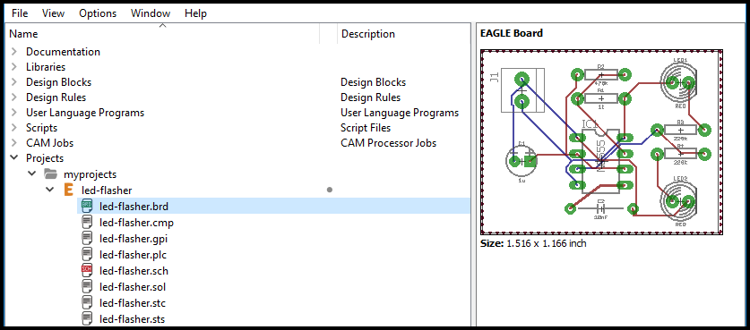
And that’s it! Just one simple press of a button and all of the Gerber files you need to send to your manufacturer have been created for you. If you head back into your Autodesk EAGLE Control Panel, you’ll see all of these new Gerber files listed alongside your existing project files.

Generating Your Drill File
While the Gerber files you just generated contain all of the details a manufacturer needs to know about your individual layers, what they don’t include is information about your drill holes. What you need now is a file that will specify the location and size of each of your drill holes. Luckily the process for making this file in Autodesk EAGLE is just as easy as making Gerbers. Here’s how:
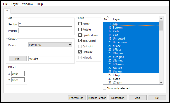
- Select the CAM Processor
 tool at the top of your interface or select File » CAM Processor to open the CAM processor dialog.
 - You now need to load a drill CAM job to get things started. Select File » Open » Job, and in your default EAGLE cam folder select the excellon.cam file, then select Open.
- You’ll now have a single Generate drill data tab available, which will grab the data from layers 44 Drills and 45 Holes, just what you need. Select the Process Job button to generate this file.

Just like all of your Gerber files, your NC Drill File will be stored in your project folder that you can access through the Autodesk EAGLE Control Panel or folder directory. Look for the .drd file, that’s the one you just made.
Time to Pack it Up
At this point, you’ve got all the files you need to send to your manufacturer to have a bare board made. The key word here being bare board. If you’re also planning to have your manufacturer assemble your components, then you’ll likely need to send some additional files like a Bill of Materials (BOM). We’ll be saving that for PCB Manufacturing Basics Part 2.
One thing to keep in mind is that while we used EAGLE’s standard Gerber CAM file to generate our documentation, some manufacturers also offer their own CAM files that you can download. When you load one of these up, they’ll provide a job template for generating Gerbers in their specific format.
Before you generate Gerber files of your own, be sure to first check with your manufacturer to see if they offer their own CAM file for Autodesk EAGLE or their preferred output format. Otherwise, you should be safe using the standard Gerber RS274-X format available in Autodesk EAGLE.
You Designed it Right, But Can You Make It?
The entirety of this blog relied on a big assumption that the design you made in Autodesk EAGLE was actually manufacturable. Sometimes this isn’t the case, whether that’s because you put silkscreen on a pad, or you have an open loop. Whatever the situation, the difference between a completed design and a design that’s ready for manufacturing can be two different realities.
SO before you ever go about sending any Gerber or NC Drill Files off to your manufacturer, we always recommend doing a thorough check to confirm that what you designed is actually what your manufacturing files show. We’ll be covering this process of validating your design in more detail in PCB Manufacturing Basics Part 3. During this validation process, you’ll also want to officially decide on what manufacturer you’d like to use. Here are a few:
- OSH Park – A great option for keeping costs low, OSH takes designs from a bunch of engineers, sticks them on one panel, and saves everyone money along the way. Their delivery timeframe is 12 days for a 2 layer board.
- Advanced Circuits – One of the biggest and well-known fab houses around in the US, these guys offer a 1-5 day delivery on boards with 1-10 layers.
- Euro Circuits – For those over the pond in Europe, Euro Circuits is another highly rated fab house that delivers within 2-7 days for 1-16 layer boards.
If you’re planning to have your manufacturer also assemble all of the components on your board, then you’ll need to create a Bill of Materials (BOM). We’ll be showing you how to do this in PCB Manufacturing Basics Part 2!
Ready to start designing and manufacturing more complex designs? Upgrade now to an Autodesk EAGLE Subscription.