Today’s Everyday App Note comes from Texas Instruments, one of the leading experts on high-speed PCB design. The PCB layout process is more important than ever as our devices require higher switching frequencies in smaller form factors. This application note addresses one of the most common problems found in a high-speed PCB layout, excessive electromagnetic interference.
Who Is This App Note For?
Any electronics designer can be working on a high-speed PCB layout; it’s all dependent on your application constraints. The problem is, there’s no hard and fast rule to determine whether your PCB is considered high speed. Here are three ways to tell if yours is:
- Specific devices. If you’re incorporating specific technologies into your layout like HDMI, PCI Express, USB, or SATA, then you’ll be dealing with high-speed issues.
- Signal integrity. If you’re encountering any kind of signal integrity or signal timing issue on your board, then it’s time to read this app note.
- Independent circuits. If the systems on your circuit all operate independently, then you have a distributed system that will likely require high-speed layout guidelines.
Why Should You Read This App Note?
Don’t let a device-specific situation determine if you should read this app note. Every electronics designer needs to read this app note. Whether you’re designing a high-speed layout now or later, EMI issues will eventually come knocking on your door. Why?
Look at the trend in electronics design and you’ll notice devices are getting faster and more tightly integrated within shrinking form factors. Every trace on that shrinking layout is going to emit some kind of EMI, and you don’t want it messing with a signal that requires precise timing from transmitter to receiver.
When a high-speed signal is disrupted in transit, the results can be catastrophic for your design. We’re talking about corrupted data, digital states that get misread, and data that gets inputted into the wrong memory address. These are not problems that you want to deal with once your product is in-field.
What Problems Does This App Note Solve?
Many variables can affect the integrity of transmission lines on your high-speed PCB layout. It’s not just about routing traces or differential signals as close as possible. You need to know about the qualities of the signals running along your traces.
This requires a deep understanding of your design, and knowledge about what parts of your circuit are prone to EMI issues. By reading this app note, you’ll be armed with fundamental high-speed layout guidelines that will help you to deal with:
- Crosstalk. This problem occurs when two tightly coupled traces influence one another. The radiation from one signal can disrupt the other, causing data corruption.
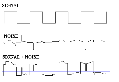
- Signal noise. This problem occurs when noise from nearby signals affect one another. Noise can lead to clock signals that don’t have a clear on/off state.
- Signal reflection. This problem occurs when a transmitted signal gets reflected back to its starting point instead of getting to its receiver. Reflection can ruin your signal timing.
This app note is divided into two sections, a high-speed design fundamentals overview and practical high-speed PCB design rules. Even if you aren’t designing a high-speed PCB layout now, it’s worth your time to read the theory section and get acquainted with this new world.
This is the start of your high-speed PCB design journey. Learn how to minimize EMI on high-speed layouts by downloading this application note from Texas Instruments now!