What Is High Speed PCB Design? An Introduction For the Complete Beginner
Is this the world of PCB design that you know? The one where you spend most of your time selecting the right components, getting them all placed on your board layout, wiring everything up with traces, and sending your files off to your manufacturer? At this stage, you’re probably designing standard boards, and if someone were to mention signal integrity, crosstalk, or reflections, you’d likely feel lost. For good reason, those aren’t the kind of problems that you solve in your day-to-day work.
But sooner or later you might have a high speed PCB project slapped down on your desk. And when this happens, you better strap on your boots, because you’ll be wading through some really deep information. The truth is, there are engineers out there with doctorates that devote their entire lives to studying high-speed PCB design, like Lee Ritchey at Speeding Edge Circuits. We are by no means trying to cover everything there is to know about high-speed design. Rather, what you’ll find within is a very basic explanation of high-speed design, written for someone that just develops regular circuit boards and wants to know what’s beyond the horizon.
So What Is High Speed PCB Design?
To put it simply, high speed PCB design is any design where the integrity of your signals starts to be affected by the physical characteristics of your circuit board, like your layout, packaging, layer stackup, interconnections, etc… If you start designing boards and run into problems like delays, attenuation, crosstalk, reflections, or emissions, then congratulations! You’ve found yourself in the world of high speed PCB design.
What makes high speed design so unique is the amount of attention paid to these issues. You might be used to designing a simple board where most of your focused time is on component placement and routing. But with a high speed design, it becomes more important to consider exactly where you are placing your traces, what width they’re going to be, how close they are to other signals, and what kind of components they are connected. And when you have to make considerations of this sort, then your PCB design process will take on a whole new level.
Now let’s back up for a moment. We know that a good indication of a high speed design is when you’re dealing with signal integrity issues, but what exactly does that mean? We need to understand signals in a nutshell.
Signals & Signal Integrity In a Nutshell
Whatever kind of design you’re working on, it’s going to be sending some kind of signal down your lengths of copper traces to a final destination. This signal can be either analog or digital, to review, here’s the difference:
Digital Signals
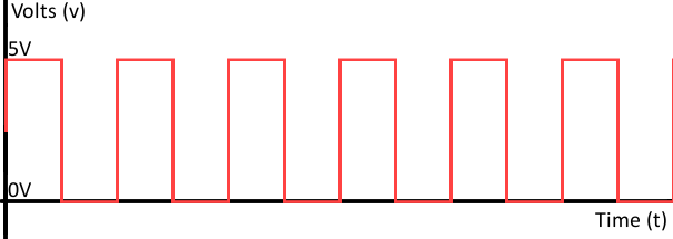
A digital signal is commonly referred to as a square wave or clock signal, and it’s what you’ll find in every digital system known to man. Unlike analog signals, which can have values all over the place, a signal provides a much simpler representation of values, consisting of a high point and low point, or 1 and 0, or on and off. If you saw a digital signal’s waveform on a graph, it would look like this:
Analog Signals
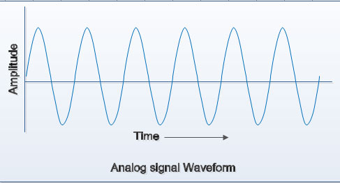
On the other side of the spectrum are analog signals, which can have a set range of positive and negative values. Unlike digital signals which are just a series of on and off points, analog signals can have a varying degree of results based on their signal strength and frequency. Looking at an analog signal’s waveform on a graph will look like this:
Now here’s the real issue with these signals, digital or analog – they are prone to interference, and this is where Signal Integrity (SI) comes into play. When a signal is affected by its environment, then issues arise. For example, let’s say that you have a net that’s transmitting some signal, which contains data, from point A to point B on your PCB layout. We can say that point A is the transmitter, and point B is the receiver of this signal. Between point A and point B, there are a ton of things that can interfere with the integrity of your signal, like:
- Signal Reflection. This is when you have a signal in transmission along a copper trace, and some of the signal gets reflected back to its starting point rather than finishing its journey to its end destination.
- Signal Ringing. This is when you have some unwanted shifting in the voltage or current on your trace, which causes extra current to flow and causes delays in the arrival of your signal at its final destination.

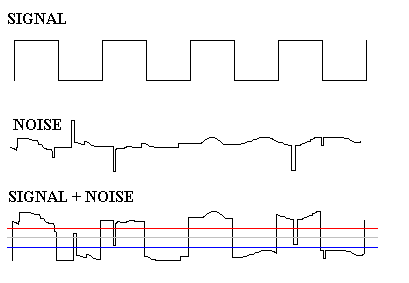
- Signal Noise. This is when you have a random fluctuation from another signal on your board, which can affect other signals in proximity to it. When there’s a lot of noise affecting a signal, then the noise can damage the signal’s data.
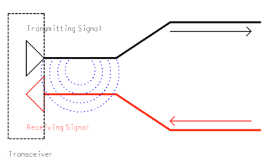
- Signal Crosstalk. This is when you place two traces or copper wires too close together, and electromagnetic radiation from one signal causes a disruption in the other signal, leading to corrupted data.
- Signal Timing. This is when you send signals traveling to their final destination, but they don’t reach it in time to line up with their clock signal. When This happens, your signal might be interpreted as a 1 when it was meant to be a 0.
Keep in mind; these five issues are just some of the many problems that can occur in a high speed PCB design. But what they all cause is the same – a disturbance in the signal that you’re trying to get from point A to point B. And when you disturb the integrity of a signal along its journey, then you corrupt the data being transmitted. As you can probably guess, your job as the engineer working on a high-speed PCB project is then to protect the integrity of all your important signals during their journey. They need to start from point A with a particular waveform and arrive at point B with the same waveform and all of their original data intact.
The Big Three Problems of High Speed PCB Design
When working on a high speed PCB design, there are a ton of issues that you’ll encounter along the way towards getting your signals interact from point A to point B. But of them all, the top three concerns to be aware of are:
- Timing. In other words, are all of the signals on your PCB layout arriving at the proper time in relation to other signals? All of the high speed signals on your board layout are controlled by a clock, and if your timing is off, then you’ll likely be receiving corrupted data.
- Integrity. In other words, do your signals look as they should when they arrive at their end destination? If they don’t, then it means that your signal likely encountered some interference along the way that ruined its integrity.
- Noise. In other words, did your signals encounter any kind of interference along their journey from transmitter to receiver? Every PCB emits some kind of noise, but when too much noise is present, then you increase the chance of data corruption.
Now, the good news is that these Big Three Problems you might encounter on a high speed PCB design can all be corrected by these Big Three Solutions:
- Impedance. Having the proper impedance between your transmitter and receiver will have a direct impact on the quality and integrity of your signals. This will also affect how sensitive your signals are to noise.
- Matching. Matching the lengths of two coupled traces will ensure that your traces arrive at the same time and in sync with your clock rates. Matching is an essential solution to look at for DDR, SATA, PCI Express, HDMI, and USB applications.
- Spacing. The closer your traces are to each other, the more susceptible they become to noise and other forms of signal interference. By not placing your traces closer than they need to be, you’ll reduce the amount of noise on your board.
How to Tell If Your Project is High Speed
There are a few schools of thought to this. But the ugly truth is that there’s no specific definition of what classifies a PCB as high speed. It really comes down to a case-by-case evaluation process. As we discussed above, if you’re encountering some signal integrity issues on your PCB layout, then that’s a good indication that you have your hands on a high speed project.
There’s also the device-specific approach. If you’re designing a motherboard, cell phone board, or DSL router board, then you’ll 100% be working on a high speed project. And if you need to incorporate specific technologies onto your layout, like HDMI, PCI Express, USB, or SATA, then know you’ll be dealing with high speed design constraints.
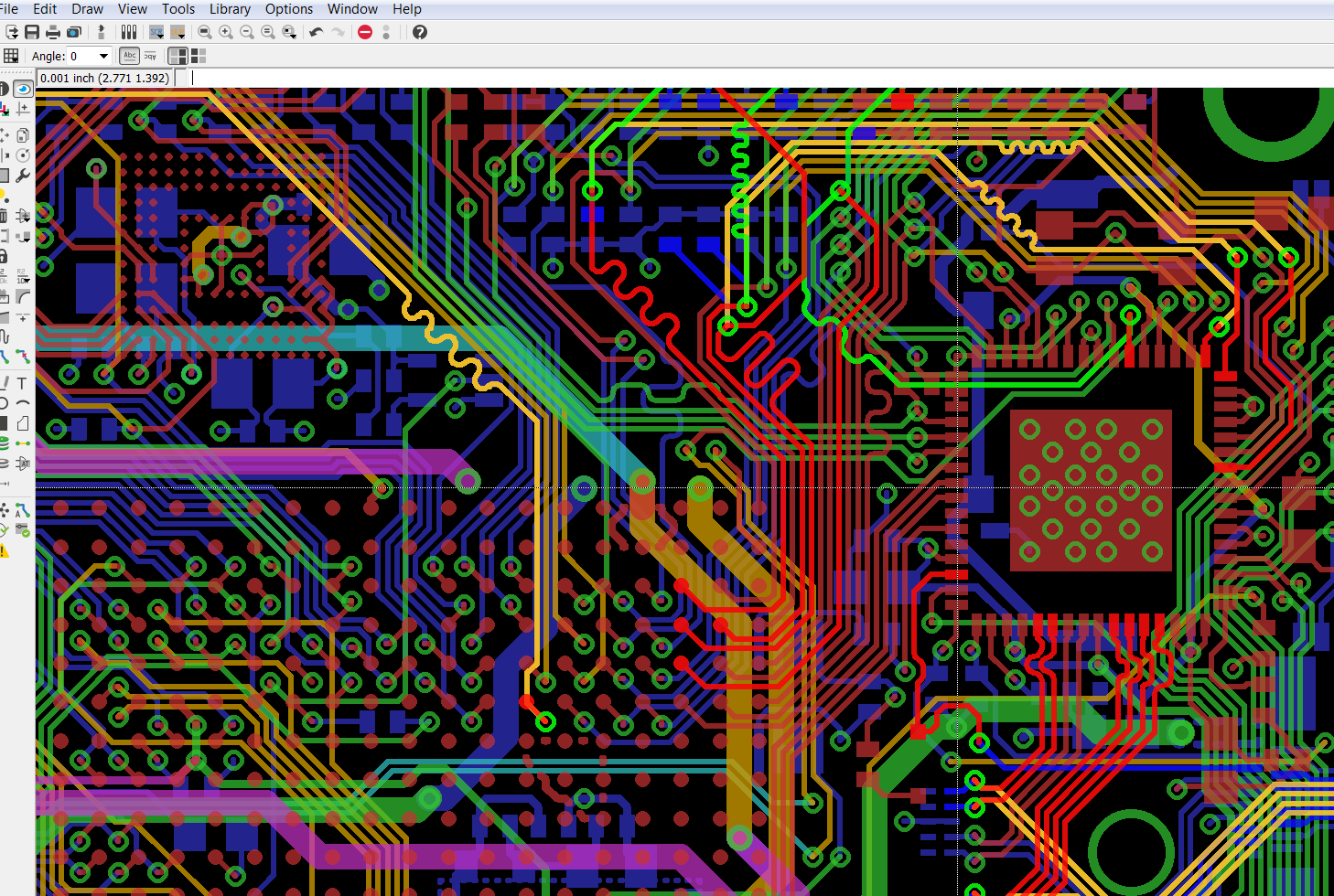
The last consideration is whether you’re working on a design that contains either lumped or distributed circuits. What’s the difference? Designs with physical systems that are all small enough that they interact together in uniform are considered lumped systems and are not high speed. But if your systems all operate independently within the confines of a greater whole, then you have a distributed system, and with that some high speed design concerns to tackle.
Here is what you should remember:
Whenever the trace length becomes a significant fraction of a wavelength of the fastest signal, you need to start looking at high speed design considerations.
This means that large PCBs start needing high speed design solutions at lower frequencies than smaller PCBs since the trace lengths are longer.
It All Starts With a Plan and EAGLE
As you can see, learning about high speed PCB design is kind of like learning about an entirely new world of engineering. EE’s end up pursuing doctorate degrees just to understand electronics at this deeper level. But what we touched on here today is merely just the surface of all the information available about high speed PCB design. What we did uncover is important – that it’s all about protecting the integrity of your signals as they journey along your PCB from a transmitter to a receiver.
If you find yourself working on a high speed design project in the future, then always remember to start with a plan before laying out anything. Take some notes on all the various design considerations you’ll have to make, like the speed of your signals, what signals need controlling impedances, how to plan out your power planes, and how all the critical points in your system will be connected. With that plan in hand, you can then start your design process! There’s a ton to learn, so journey forth, and don’t be afraid to research along the way as you define your board layout, place your components, and precisely plan your routes.
Ready to get started with your first high speed PCB design project? Try Autodesk EAGLE for free today!