High-speed PCB design is any design where the integrity of your signals starts to be affected by the physical characteristics of your circuit board, like your layout, packaging, layer stack up, interconnections, etc. In Part 1 of this three-part series, let’s take a look at how to determine when you have a high-speed PCB design.
High-speed PCB design requires that you know the frequency of the signals you’re routing. The higher the frequency, the more things like trace length and impedance matter. Stub length (short traces branching off longer traces) also begin to matter. Cross-talk, EMC (Electromagnetic Compatibility), and EMI (Electromagnetic Interference) issues also begin to show up with higher frequencies.
In this series, we’ll look at the challenges high-speed designs present and how to minimize the effects on signal integrity (SI) and power integrity (PI). So, how do you know when you’ve got a high-speed design?

High Speed = High Frequencies
If you’re working with rf (radio frequencies) you’re dealing with high frequency. Any wireless interface (e.g., IEEE 802.11) is going to have high frequencies. But exactly what frequencies are considered high frequency?

Well, the answer to this question is – high frequency or high-speed designs involve frequencies that begin to exhibit the effects we mentioned earlier (cross talk, EMC/EMI) and signal integrity issues such as reflections due to impedance mismatches and timing differences due to uneven trace lengths. This happens with frequencies around 50 MHz, but remember, this is a generalization, cross-talk, EMI/EMC, and other problems can occur at lower frequencies.
High-Speed PCB Design | Rise Time and Frequency

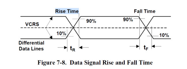
The rise time of your signals plays a huge role in the frequencies you need to factor into your designs. The faster your signals change, the higher their frequency content (and the more you have to worry about all the problems associated with high frequencies). A common formula used to determine the highest frequency present in your signals is: 𝑓=0.35/𝑡𝑟
Where 𝑓 = highest frequency of concern and 𝑡𝑟 = rise time of your signal. Consider a microcontroller general-purpose pin that takes 6 ns to transition from low to high. The highest frequency generated that we would concern ourselves with is: 𝑓=0.35/𝑡𝑟=0.35/6 𝑛𝑠=58𝑀𝐻𝑧
The problems associated with high-speed designs may begin to appear if you forget to follow the techniques outlined in this series.

You might think a USB 2.0 interface in low-speed mode would not require high-speed techniques as low speed is only 12Mb/s, but consider that 𝑡𝑟 is between 4 ns and 20ns which means that frequencies present on your USB traces could be as high as 87.5 MHz. USB 2.0 high-Speed mode is definitely in the area of high-speed design as 𝑡𝑟= 500 ps, meaning frequencies of 700 MHz will be present.
Cross talk, EMI, and EMC issues more easily exhibit themselves with high-speed signals. Impedance of traces and impedance matching must be handled correctly in high-speed designs. To determine whether your PCB requires high-speed design considerations, consider not only the frequencies of your signal but the rise time of the signal as well. Be wary if the frequencies start creeping into the > 50 MHz zone.
View the rest of the series here:
- High-Speed PCB Design Part 2: What to Consider First
- High-Speed PCB Design Part 3: Avoiding Signal Integrity Issues
Ready to start with high-speed PCB design? Get started with the Fusion 360 Signal Integrity Extension today.
