High-speed PCB design is any design where the integrity of your signals starts to be affected by the physical characteristics of your circuit board. For Part 2 of this three-part series, let’s take a look at some top factors to consider when laying out a high-speed PCB.
The first thing to consider before laying out a high-speed PCB is the layer stack-up. Make sure each signal plane is immediately next to a ground plane to prevent electric fields from interacting with each other. To learn more about layer stack-ups, check out: PCB Layer Stack Fundamentals Part 1: Using Multiple Copper Layers.
High-Speed PCB Design: Choosing a Substrate Material
FR4 is the most common PCB substrate and is good up to around 1 GHz. Above this frequency and if routes begin to extend into the 10” or longer range, selecting a substrate with better material properties may be needed. Work closely with your contract manufacturer during this stage. They can tell you what they have done before that works for the frequencies and trace lengths present in your design. Substrates suited for multi-GHz designs have lower DFs (Dissipation Factors). This results in less signal loss and more uniform Dielectric properties, which can cause more consistent impedances. They often can have better thermal characteristics too. However, they are more expensive.
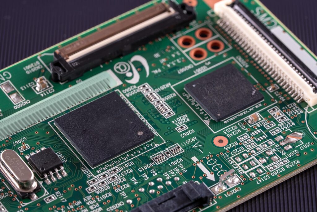
High-Speed PCB Design: Grouping
Next, group your components into their appropriate sections and place all the “must-go-here” components onto the PCB.
After you’ve done this, you can begin to look at high-speed signals and how they should be routed. High-speed communications and interface standards commonly used in consumer products such as High-Speed USB, High-Speed Ethernet, and Antenna feeds all need controlled impedance routes. High-capacity memory and display products such as DVI, HDMI, PCI-e, and DDR require these high-speed techniques.
High-Speed PCB Design: Microstrip and Stripline
You have two options for impedance-controlled traces: stripline and microstrip:

Stripline and microstrip are often used for differential signals. Fusion 360 Electronics can display the impedance of your traces.
Routing Considerations
Any time you lay out PCBs, the goal is always to keep the trace as short as possible. This is especially important when routing high-speed signals, as the time it takes for a pulse to travel from a transmitting gate to receiving gate may differ enough from trace to trace to cause timing issues. In fact, high-speed interface design specifications require that lines are of the same length. It’s for this reason that we meander signals. This ensures the same electrical length is present on the traces and that signals, therefore, arrive at the same time.
Using mitered traces or rounded traces at a 90° angle introduces impedance changes. The result – reflections of signals that can cause signal loss or degradations.

High-Speed PCB Design Part 3: Avoiding Signal Integrity Issues
View the rest of the series here:
- High-Speed PCB Design Part 1: How To Identify a High Speed Design
- High-Speed PCB Design Part 3: Avoiding Signal Integrity Issues
Ready to get started with high-speed PCB design? Try the Fusion 360 Signal Integrity Extension.