Explore the essential rules and guidelines for designing medical PCBs, focusing on critical design guidelines, thermal management techniques, quality control, and reliability testing.

In healthcare technology, the design and manufacture of medical PCBs (Print circuit boards) is a pivotal processe to ensure the functionality and reliability of medical devices. These components are the backbone of myriad medical innovations, from advanced diagnostic machinery to portable monitoring devices, making the integrity of their design paramount.
The significance of medical PCBs extends beyond their technical roles. They are integral in complying with stringent medical device regulations, ensuring patient safety, and maintaining the efficacy of medical treatments. Understanding the nuances of medical PCB design, including adherence to FDA compliance and medical device classification is critical for engineers and designers.
This article will guide you through essential rules and guidelines for designing medical PCBs. We’ll focus on critical design guidelines, thermal management techniques, quality control, and reliability testing. Additionally, it will highlight the importance of simulation tools in optimizing the design process and ensuring medical device safety.
You’ll gain insight into how adherence to medical device regulations and careful consideration of medical device classification can significantly impact the functionality and reliability of medical PCBs. Whether you are new to the field or looking to refine your design practices, this roadmap offers valuable knowledge to navigate the complexities of medical PCB design.
Medical PCBs – critical design guidelines
SMD vs. PTH components

Choosing between Surface Mount Technology (SMT) and Plated-Through-Hole (PTH) technology is crucial when designing medical PCBs. Although PTH mounting is still used for applications like power supply boards or when multiple connectors are required, SMT is generally preferred in medical applications. The advantages of SMT include utilizing smaller components, which reduces the PCB size and increases component density. This cuts down on costs and speeds up the assembly process since no drilling is required for SMD components. One of the smallest SMD packages available is the 008004. It measures just 0.25mm x 0.125mm, exemplifying the miniaturization achievable with SMT.
Trace width and spacing

The design of trace widths and spacing is dictated by the specific requirements of the medical PCB. It focuses on balancing factors like cost, board density, and performance. For high-density designs, technologies such as High-Density Interconnect (HDI) are often employed, allowing for more interconnections and smaller via sizes. This includes using via-in-pad technology, which is particularly beneficial for components with a high pin count and narrow pitch.
Trace specifications also play a pivotal role in ensuring the functionality and safety of medical PCBs. For instance, high-speed USB lines require careful consideration of trace width, spacing, and length to minimize signal degradation and interference. Similarly, power traces need to be wider to effectively handle higher currents and prevent issues like overheating or electrical arcing. Controlled impedance routing and selecting appropriate trace widths are essential for meeting both performance standards and regulatory compliance.
Adhering to these guidelines, ensures that your medical PCB design is efficient and compliant with the stringent standards required.
Medical PCBs – thermal management techniques
Heat dissipation methods

Ensuring effective heat dissipation is crucial to maintaining device reliability and performance when designing medical PCBs. One common technique is heat sinks. These thermally conductive metallic parts designed to dissipate heat over a large surface area. They are typically attached to heat-producing components to facilitate heat transfer away from critical parts of the PCB.
Additionally, cooling fans may introduce a stream of cool air, especially in high-current power supplies. This method enhances heat removal efficiency, preventing heat accumulation that could lead to component failure.
Incorporating thick copper traces for PCBs in high-power applications can significantly improve heat distribution. The copper’s increased surface area facilitates better heat dissipation across the PCB.
Heat pipes offer an innovative solution in tight spaces where traditional methods may not be feasible. These utilize a fluid that absorbs heat, transitions to vapor, and circulates within the pipe to a condenser, dissipating heat before returning to liquid form. This continuous cycle effectively manages heat in compact devices.
Materials like polyimide for Flex PCBs or aluminum for metal core PCBs can also enhance heat dissipation. These are chosen for their ability to transfer heat efficiently to cooler regions of the boaard to prevent hot spots.
Thermal simulation
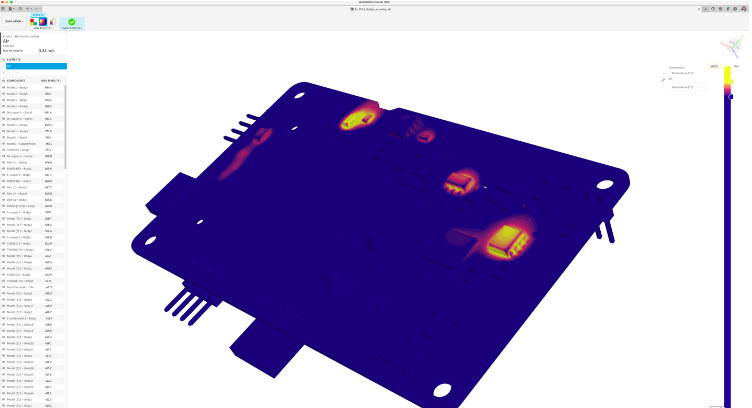
Thermal simulation plays a pivotal role in ensuring the effectiveness of these heat dissipation methods. This process uses software tools to model heat flow and temperature distribution within the PCB during operation. Simulating different thermal scenarios allows you to identify potential hot spots and adjust the design accordingly to optimize heat management.
Thermal simulation software can validate your design by predicting how heat will move through the substrate and components. This is crucial for determining the right combination of heat dissipation methods and ensuring that the temperature remains within safe operational limits throughout the PCB.
Using thermal simulation also allows for the adjustment of component layout to avoid the formation of hot spots. It also ensures that heat is directed towards parts of the board that can handle higher temperatures. This strategic placement is essential for maintaining the integrity and functionality of medical PCBs.
By integrating these thermal management techniques and leveraging advanced simulation tools, medical PCBs can be designed that meet the required performance standards and adhere to strict medical device safety regulations.
Medical PCBs – Testing and Debugging

Test points placement
When designing medical PCBs, strategically placing test points is critical for effective testing and debugging. Test points are essential elements that should be included during the PCB design phase. These are exposed metal pads on an exterior layer of the board, connected to a net, allowing probes from automated test equipment to conduct tests. Two primary types of test points are used in PCB designs: fabrication test points for manual testing and assembly test points for automated testing equipment. Fabrication test points often have a post soldered into them to facilitate clipping on a test probe. Assembly test points accommodate the probes of automated test systems.
The placement and management of these test points are crucial. PCB design tools often come equipped with features that allow designers to set parameters for test point placement, such as proximity to each other and additional design rules for various tests. Once parameters are set, test points can be assigned manually or automatically and iteratively. Ultimately, ensuring they comply with the design rules.
Debugging methods
Debugging a populated PCB requires a systematic approach to identify and resolve issues. Initially, conducting a visual check of the board is beneficial to spot any obvious problems like open or short connections. If issues persist, using an oscilloscope to check each pin of the IC for correct voltage levels can be invaluable. This tool is essential for verifying that the oscillator is functioning correctly and that the IC receives the correct clock signals.
For more complex debugging, techniques such as employing a current-limited power supply during initial tests can prevent damage from potential shorts. Thus allowing quick disconnection if issues arise. Checking power supply rails for correct voltage levels is also critical in debugging.
In cases where intermittent faults occur, using thermal detection methods like a can of Freeze-It can help localize the faulty component or connection. Additionally, ensuring proper grounding and employing techniques to shield the circuit from external electromagnetic noise can mitigate issues that disrupt circuit functionality.
By integrating these strategic test point placements and comprehensive debugging methods, you can enhance the reliability and functionality of medical PCBs. This ensures they meet the stringent standards required in medical applications.
Medical PCBs – simulation tools
Digital twin technology

Digital twin technology is revolutionizing the design and operation of medical PCBs. This technology creates a virtual model that mirrors the physical circuit throughout its lifecycle. This technology incorporates historical and real-time data, allowing for proactive decision-making and lifecycle management. For instance, digital twins can simulate the entire operation of a medical device. This is acheived by integrating data from embedded sensors to monitor the device’s health and predict maintenance needs before failures occur. This predictive maintenance approach not only enhances device reliability but also ensures patient safety by minimizing the risks of device failure.
Benefits of simulation
Implementing simulation techniques, particularly digital twins, significantly reduces development costs and accelerates the time-to-market for medical-grade PCBs. By identifying potential design errors early in the development phase, digital twin technology allows for quicker iterations and design process optimization. Moreover, thermal simulations can detect hot spots under various operational conditions, enabling adjustments to the schematic that prevent costly and time-consuming reworks post-production.
Furthermore, digital twins play a crucial role in device development’s verification and validation (V&V) stages. They enable detailed analysis of how devices will perform under realistic anatomical conditions, thereby reducing the risk of device failure post-market and supporting more substantial regulatory submissions. This ensures compliance with medical standards and contributes to significant cost savings and a faster commercial launch.
With Autodesk Fusion, you gain valuable insights into the thermal performance of your electronics designs through its Ecooling simulation capabilities, optimizing heat dissipation and ensuring reliability. Additionally, the Autodesk Fusion Signal Integrity Extension empowers you to analyze and validate the high-speed signal behavior of your PCB designs, mitigating potential signal integrity issues and enhancing overall performance.
Conclusion
Throughout this exploration of medical PCB design, we have journeyed through the essential practices and considerations that ensure the functionality and reliability of medical devices. The complexity of designing medical PCBs has unfolded from critical design decisions like choosing between SMD and PTH components to place test points for efficient debugging strategically. Further accentuated by the importance of thermal management techniques and the leverage of digital twin technology, we’ve established that successful medical PCB design is both an art and a science, requiring meticulous attention to detail and an unwavering commitment to regulatory compliance and safety.
The take-home message is clear: the stakes and demands are high in the fast-evolving landscape of healthcare technology. By adhering to these guidelines, designers can ensure that their medical PCB projects meet and exceed expectations regarding quality, reliability, and regulatory adherence. As we look toward the future, continuous innovation in this field promises to enhance the capabilities of medical devices and open up new possibilities for medical treatment, emphasizing the pivotal role of medical PCB design in advancing healthcare technology.
Autodesk Fusion equips you with the essential tools to address all your electronic design requirements. You can streamline your workflow and enhance productivity by utilizing the intuitive design rule settings for material layer assignment and smart outputs. Discover the innovative features and functionalities that will revolutionize how you approach electronic design. Experience a new era of design by trying Autodesk Fusion today.