This post is also available in: Deutsch (German) 日本語 (Japanese)
Let’s take an in-depth look at the differences between Gerber and ODB++ manufacturing files and how to export them in Autodesk Fusion.
Before reading this blog, take a look at the article regarding layers in Autodesk Fusion. Here, you will learn the intended use of every layer, which can be relevant when exporting your design manufacturing file.
The two most commonly supported manufacturing files by PCB prototype houses and manufacturing companies are Gerber and ODB++. Let’s discuss the differences between the two.
Differences between Gerber and ODB++ manufacturing files
Gerber files
Gerber files originated in the 1960s as a proprietary format created by Gerber Systems Corp. to control the photoplotters used in PCB manufacturing. These files act as detailed blueprints for each circuit board layer, including copper traces, solder masks, and drill holes. 1998, the Extended Gerber, or RS-274X format, became the industry standard due to its human-readable structure and improved functionality. Today, PCB manufacturers worldwide use Gerber files to fabricate circuit boards from design files accurately.
ODB++
ODB++, initially developed by Valor Computerized Systems in the mid-1990s, aimed to streamline printed circuit board (PCB) design data exchange. Initially a proprietary CAD-to-CAM format, it evolved to include component information, hence the “++” suffix. In 2008, the XML-based version of ODB++ was donated to IPC, leading to the development of the open IPC-2581 standard. Today, ODB++ is the industry standard for PCB manufacturing data exchange, facilitating communication between designers and manufacturers by providing a comprehensive package of design and manufacturing data in a single file.
Autodesk Fusion supports both Gerber and ODB++ manufacturing files, but which one is better?
Both Gerber and ODB++ are widely used in PCB manufacturing. Gerber, the older format, is more universally accepted and focuses on the physical board layout. ODB++ is a newer, more comprehensive format with additional design and manufacturing data, making it better suited for complex designs and integrated workflows. While Gerber remains more prevalent due to its long history, ODB++ is gaining popularity, especially for advanced projects that require seamless data exchange between different tools. The choice between them often depends on the design’s complexity, the project’s specific needs, and what the manufacturer prefers.
Generating PCB manufacturing files
TIP: Before producing your PCB manufacturing files, carefully review any design error violations by running the DRC in the manufacturing tab. If any errors or warnings are acceptable, make sure you tag them as such to save time.
You must be aware that the manufacturing file is NOT one file. It is an arrangement of files based on layer combinations. For example, the top layer of your PCB, AKA your component side, will consist of the top copper, pad, and via layers. This table will put it all together for you. Our table is an example of the manufacturing files for a 4-layered board: two exterior copper and two internal copper layers.
Gerber files
| Name | Fusion Name | Layer Combination |
| Top Copper | Copper_Top_L1.gbr | Top, Pads, Vias (1, 17, 18) |
| Copper Layer 2 (Internal Layer) | Copper_Inner_L2.gbr | Route2, Pad, Vias (2, 17, 18) |
| Copper Layer 15 (Internal Layer) | Copper_Inner_L15.gbr | Route15, Pad, Vias (15, 17, 18) |
| Bottom Copper | Copper_Bottom_L15.gbr | Bottom, Pads Via (16, 17, 18) |
| Profile | Profile.gbr | Board Shape, Cutouts |
| Soldermask Top | Soldermask_Top.gbr | SolderMaskTop (29) |
| Soldermask Bottom | Soldermask_Bottom.gbr | SolderMaskBottom (30) |
| Solderpaste Top | Solderpaste_Top.gbr | StencilTop (31) |
| Solderpaste Bottom | Solderpaste_Bottom.gbr | StencilBottom (32) |
| Silkscreen Top | Silkscreen_Top.gbr | SilkscreenTop, NamesTop (21, 25) |
| Silkscreen Bottom | Silkscreen_Bottom.gbr | SilkscreenBottom, Names Bottom (21, 25) |
| Additional Files Generated | ||
| Drill File (Excellon 3.3 Format) | Design_File_Name.xln | Based on Layers 44 and 45 |
| Bill of Material | Design_File_Name.txt | Extracted from Schematic |
| Pick and Place Top | Design_File_Name_Front.txt | Extracted from PCB Top Reference |
| Pick and Place Bottom | Design_File_Name_Back.txt | Extracted from PCB Bottom Reference |
The naming convention established here will change slightly when we get to the section about ODB++ output. For now, let’s stick to Gerber outputs and generate additional files.
Fusion manufacturing file generation, click by click
2 clicks and done for Gerber files
By adhering to our standardized layer formats and functionalities detailed in the Layers blog, you can streamline your workflow and generate “Gerber, NC Drill, Assembly, and Drawing” with only one click directly from the manufacturing tab. This option will automatically load a CAM job based on your Layer stackup. Our example shows that the CAM-loaded template for four layers.
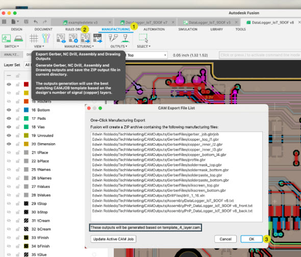
The file with the extension .gbrjob is referenced as a job file. This file remembers the settings used to generate your Gerber files. It is convenient to have this available just in case you need to re-create your manufacturing files again using the same parameters you have set up.
Fusion open data base output, click by click
2 clicks and done for ODB++
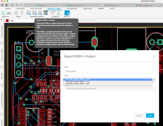
Similar to what we did with Gerbers, select the manufacturing tab and choose the option “Export ODB++ Output” option. You will notice the type of compression you can use in the dialog box. Selecting save will prompt you to indicate where to save the manufacturing files locally. After choosing the target local folder, the manufacturing files in ODB++ format will be exported. The output will include compressed formats in .tgz and .tar and a non-compressed version of the files. Before generating the output files, check with your board or prototype manufacturing to see their preferences. Most Gerber Viewers support ODB++; if you are new to generating PCB manufacturing files, I recommend you get one and check your manufacturing files. Check with your manufacturer; is it possible they offer a free viewer or will recommend one they prefer for you to use.
Fusion CAM processor: Gerber and ODB++ manufacturing files
Customize outputs
You must use the CAM processor if you have used any layers differently than intended or created a layer you wish to be part of our manufacturing PCB files. The CAM processor will initially load using a default template based on your layer stackup, which can be easily modified in the CAM Processor. From the PCB Workspace Manufacturing tab, let’s go ahead and select the CAM processor icon.
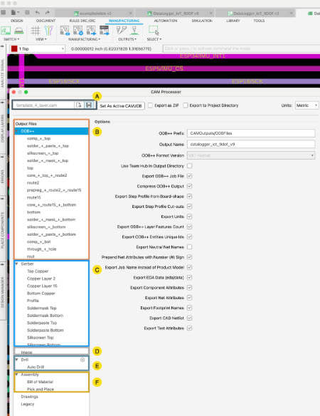
The CAM processor has many parameters, so I will do my best to explain them in the easiest way possible. Yes, the CAM processor will simultaneously generate the Gerber and ODB++ files.
CAM processor dialog box
Let’s go ahead and unpack sections of the CAM processor dialog box.
A. This is the default CAM Processor job that is loaded, which is based on your DRC layer stackup.
B. This section is for the ODB++ output. With the header highlighted, you can change the intended output. parameters. I recommend that you don’t make changes here unless recommended by the board manufacturer. Our defaults were carefully established based on manufacturers’ recommendations.
C. This section is for Gerber files, another commonly used PCB Manufacturing file format. The sub-sections match the One-Click solution we explained earlier regarding combining layers for Copper Top, Copper Bottom, etc.
D. Use the Image section to include images the manufacturer can reference in your PCB.
E. The Drill section will generate the files necessary to drill or poke all the holes on your PCB. The default format is excellon: 3.3, with no leading zeros.
F. The Assembly section will consist of 3 files, your BOM, and the Pick-and-Place for components on the top and bottom layers.
You can modify the format of the files to export by clicking the section’s title. Only make changes if recommended by the board manufacturer.

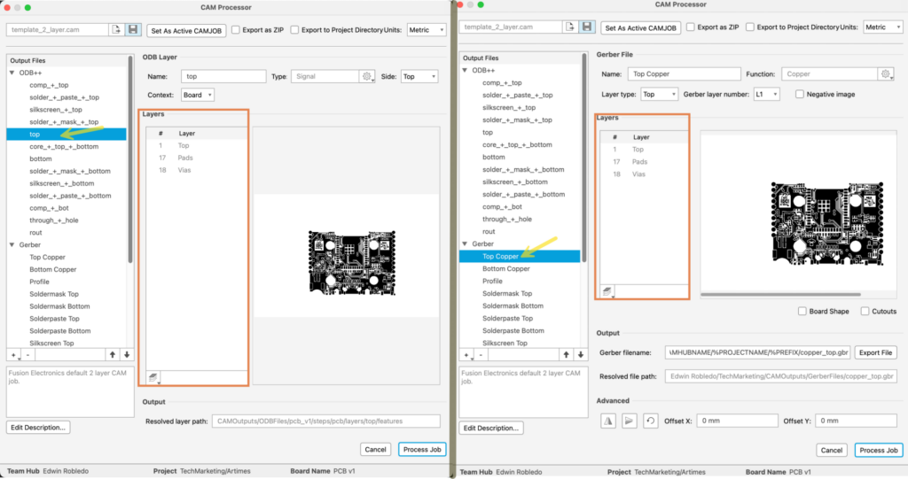
Selecting the sub-section will provide an image preview with the current selected layers. Not all subsections of the ODB++ section will have a preview image since they carry parameter details of the PCB that do not need to be previewed.
Additional parameters
In addition to the preview, you will notice some additional parameters you can change, such as the file’s destination, the name of the output file, and other parameters. When processing the job, a prompt will occur to provide a destination.
Notice that I have highlighted the section regarding the layers selected for the Top Copper layers. Notice that both have the Top, Pads, and Via chosen layers. The combination of all these layers will create the top copper side of the board. This layer combination will rarely be altered. I strongly suggest only placing any assets in this section intended to be copper on the component side of the board. If you select an additional layer, you run the risk of Short circuits.
Modifying layer stackup
For my following example, let us modify the Layer stackup. That way, you can see how layers can influence your output.
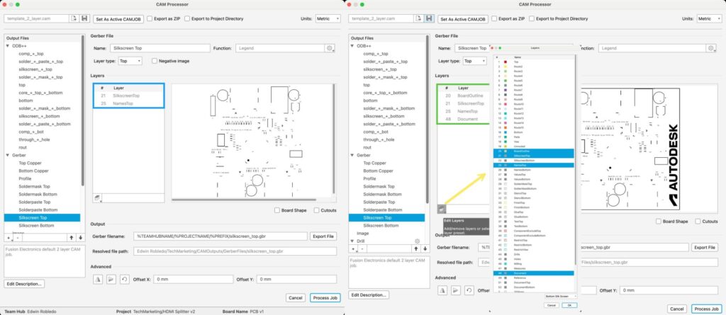
By default, the top silkscreen output will include the SilkscreenTop layer combined with the component reference designators on the NamesTop layer. My manufacturer has indicated they would prefer I include the board outline on all my output files, and they have no problem placing the company logo.
I will select the layer stack option in the CAM processor and include the BoardOutline and Document layers, which I used for the Company Logo. Notice that the preview window will adapt.
This is why clearly understanding of each layer’s function is paramount. This empowers you to manipulate your output manufacturing files easily. If necessary, you can also add subsections for additional manufacturing details.
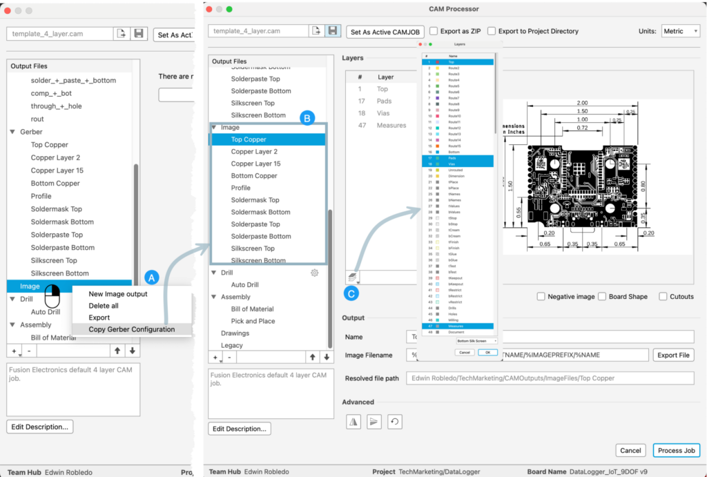
For the following example, I want to leverage the Image section to include the measurement of my board, which will be used for reference when verifying the dimensions of my PCB. I will right-click the Image section and select the Copy Gerber Configuration option (A). All my images will adopt the same subsection setup as the Gerber file (B). By highlighting the Top Copper section, I can now add the Measure (Layer 47) layer (C) to the image that will be exported. The images can be exported in BMP, JPG, PDG, or PNG.
Now that the CAM processor has been set up using you and your manufacturer’s preferences select “process job” to generate all your manufacturing files. After selecting your local folder, click OK. The ODB++, Gerber, Image, and information files will be in different folders. There will also be a file with the extension .gbrjob, which contains all the parameter changes you have selected for this CAM process.
Export Gerber and ODB++ manufacturing files in Autodesk Fusion
Autodesk Fusion electronic design has all the tools required to design and export your files for manufacturing successfully. Its easy interface and flexibility of use make it a perfect tool for your next project. Why not try it today for free and experience its design capabilities combined with collaboration capabilities? You’ll get your product done better and more efficiently, saving time and resources.