Nobody likes the headaches that happen during PCB manufacturing. But there are many things you can do to ensure your PCB manufacture goes smoothly. Follow this PCB manufacturing advice, and your PCBs will cost less, have fewer production failures, and overall better quality.
BOM management
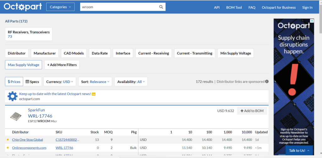
If the recent pandemic has taught us anything, it is the fragility of the supply chain. You can’t manufacture your product if you can’t get the needed components. Minimize your risk by using a standard set of easily obtainable parts and include alternative equivalents whenever possible. Try to use popular parts and part values when you can. Popular parts are popular for a reason – they’re easy to source, and lots are available. Check online supplier databases and aggregators like Octopart and look for features that are always in stock in large quantities. Lastly, stay away from end-of-life and obsolete parts.
Minimize through-hole components
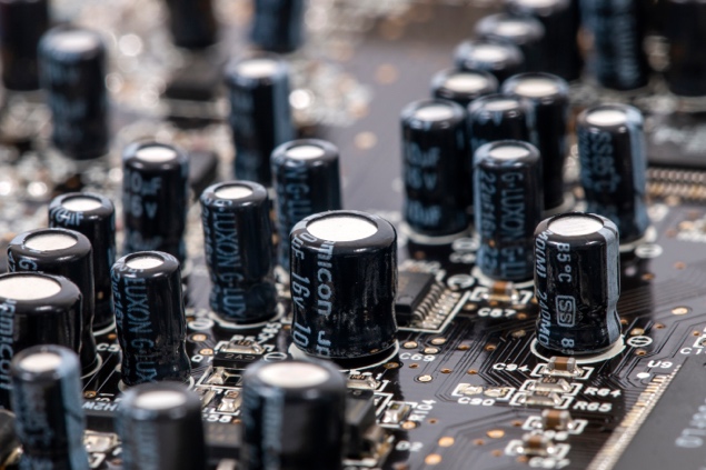
Through-hole parts are generally more expensive than surface mounts. They don’t easily work with surface mount pick and place machines, and manufacturers find they must manually install and solder them. This, of course, costs more and can introduce human errors.
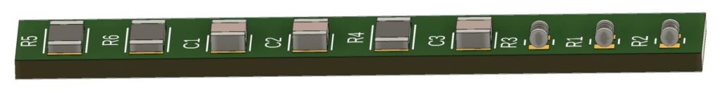
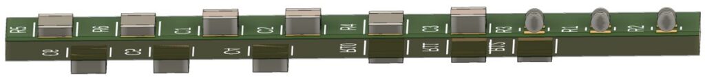
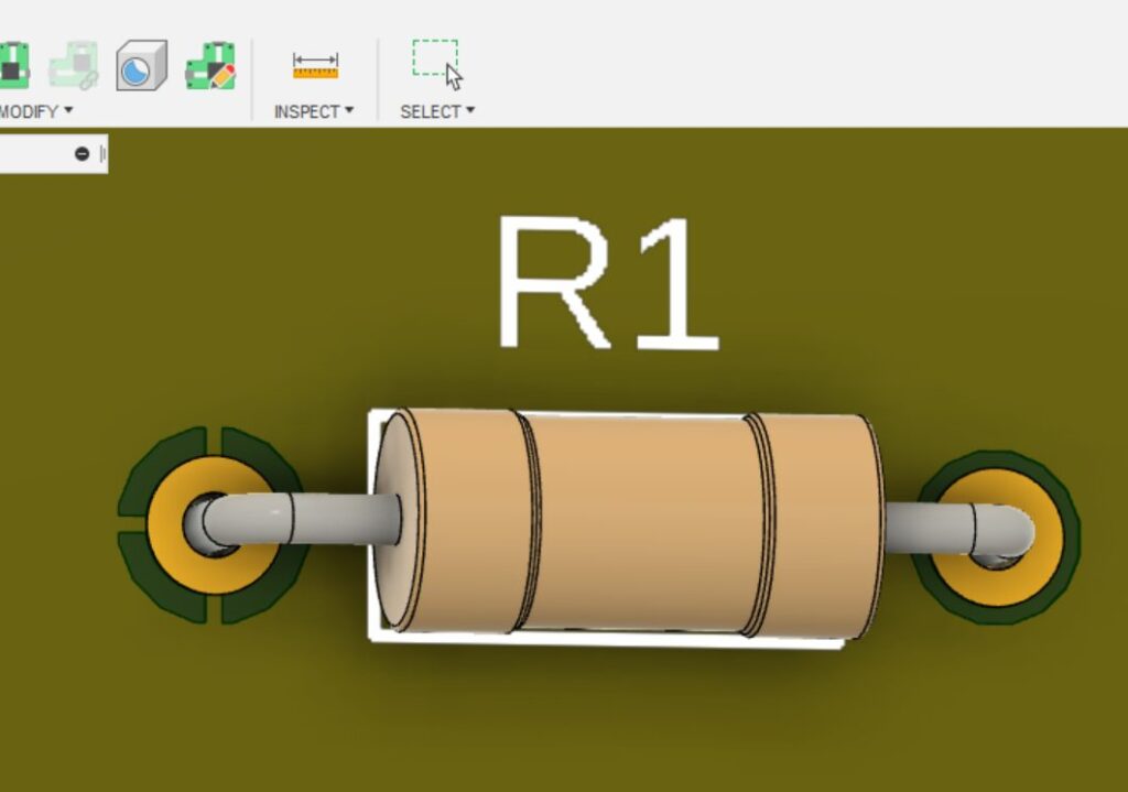
Connectors are common THT (Through Hole Technology) parts and are a source of many manufacturing headaches. Repeated insertion of connectors into their mating part will eventually fail. Try to minimize their use and use an SMT part if you can.
Know your manufacturer’s capabilities
Asking your CM (Contract Manufacturer) to do something they’re not able to is silly. But even if they can do it doesn’t mean you should ask them. Don’t use tiny holes or traces if not needed. They’re more expensive, and if on, the outer layers are easily damaged.
Knowing what your CM charges can help you make decisions to minimize costs. Cost mitigation always makes PCB manufacturing easier, resulting in cost savings and increased quality.
Try to get all your components on one side. Placing components on both the top and bottom of your PCB requires extra assembly steps and introduces more chances for assembly errors.
Provide thermal relief
Large sections of copper on your PCB suck heat away during the soldering process and can result in cold solder joints – something nobody wants. Ensure adequate thermal relief for THT connections that attach to large areas of copper like ground or power planes.
Make sure your spokes are thick enough to handle the total current flowing to the ground from your component.
Poka-yoke your PCB
Poka-yoke is a term coined by Shigeo Shingo in the 1960s. He realized that quality could be guaranteed by designing manufacturing processes to only run successfully or if done incorrectly, were obvious to the operator. It’s a similar term to “foolproofing.”
Use keyed connectors so that connectors can only be plugged in one way.
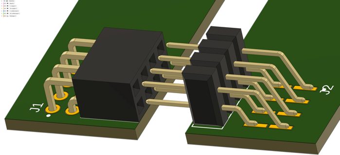
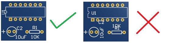
Stagger mounting holes so that boards can only be mounted in one position. Make sure your silkscreen identifies the orientation of diodes and pin one on ICs.
CMs will tell you that a large source of their assembly problems is due to missing or incorrect orientation marks. Whenever possible, make an assembly error stand out like a sore thumb.
Leave enough room
Sometimes it can be hard to leave enough room to squeeze every last component. CMs don’t like crowded parts on PCBs as they introduce the possibility of shorts and other assembly errors and increase costs.
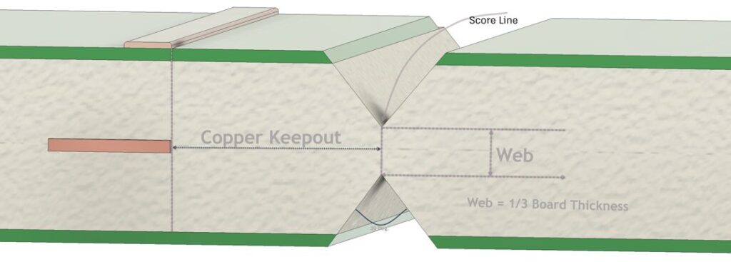
Keep traces well within the PCB edge. 10mil for outer layers and 15mil for inner is a good starting point. Keep components away from the board edge as well. Components close to the board can crack or be damaged during the de-paneling process.
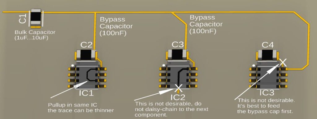
Another good tip is to place and route bypass caps immediately after placing the required components. Don’t make your life difficult by trying to shoehorn them in after everything else has been placed.
And speaking of bypass capacitors, make sure you place them close to their IC and route power to the IC after the capacitor.
Silkscreens
Keep silkscreen graphics off of pads. Follow your CM’s guidelines for minimum font size and line width. 50mil height and 6mil linewidth are good starting points.
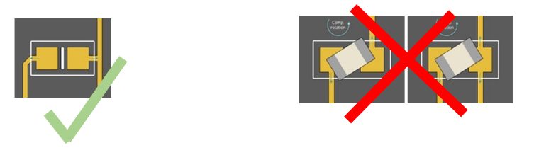
Minimize tombstoning
Tombstoning is the lifting of one pad of an SMD during reflow soldering.
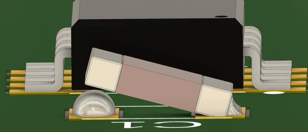
It’s caused by pads heating unevenly due to traces not exiting a pad evenly. You can prevent misalignments and tombstoning by ensuring that pads heat evenly.
Fit
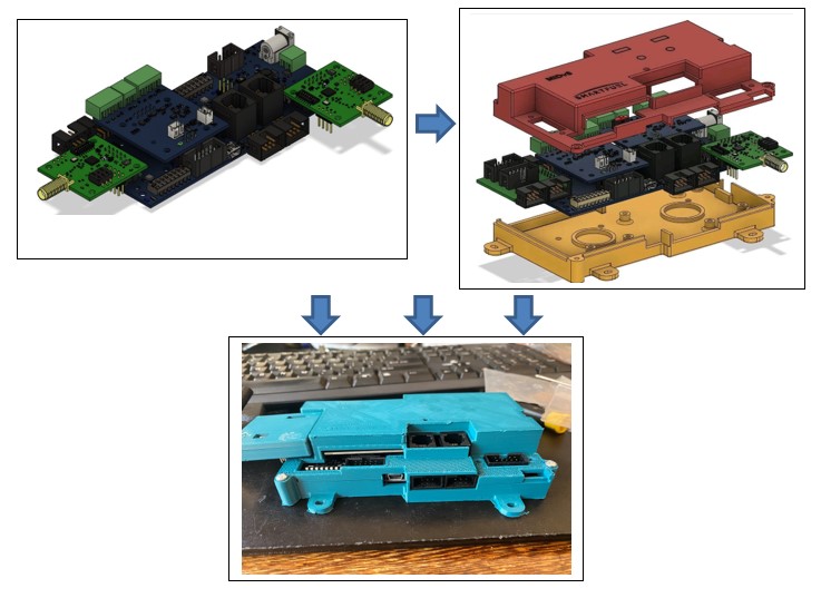
Lastly, make sure your PCB fits into your enclosure. Autodesk Fusion 360 makes it easy to see collisions of PCB with enclosure walls and makes it easy to move components out of the way of enclosure obstructions.
We hope these PCB manufacturing tips make your next project more manageable. Try Autodesk Fusion 360 for free today for an integrated CAD, CAM, CAE, and PCB solution: