
Logic gates are the fundamental building blocks of digital electronic circuits. They follow Boolean Algebra rules, which are very easy to understand and implement for everyone—including beginner-level designers. They help circuits make decisions, so they form a significant chunk of the microprocessor and microcontroller circuitry.
Essentially, there are seven types of logic gates, out of which we have discussed three (AND, OR, NOR) in the previous blog post. In this blog post, we will cover the following gates and see how they work when incorporated in digital circuits:
- NOT
- NAND
- XOR
- XNOR
By the end of this post, you will be able to perform various mathematical operations using logic gates and build useful circuits that use multiple logic gates’ features.
NOT Gate
NOT gate is, by far, the simplest logic gate because it performs the fundamental function of inverting, which is why a NOT gate is also called an Inverter. What does a logic inverter do?
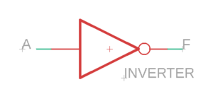
A logic inverter, or a NOT gate, inverts the logic level present on its input terminal. For instance, if there is a ‘1’ on a NOT gate’s input, it will generate a ‘0’ as the output and vice versa. NOT gate is the only gate with a single input terminal, while all the other gates have two or more input terminals. The Boolean equation for a NOT gate can be given as follows:
F=A
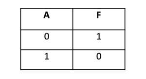
Which generates the following truth table:
Internal Working
We can use resistors and transistors to represent the internal working of a NOT gate. The transistor base acts as the input terminal, while the output is measured from the collector terminal. The circuit is designed, as shown in the diagram below.
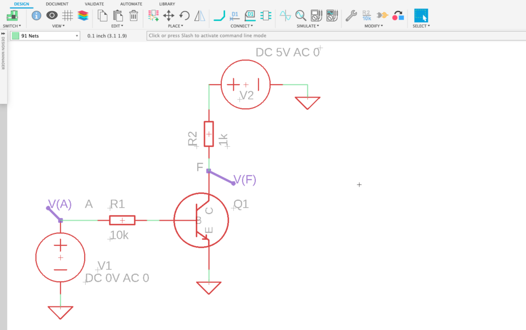
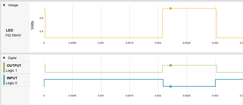
Voltage probes are used to measure the logic level at the input and output terminals. V(A) represents the point where the input signal is measured, while V(F) represents the output terminal. As you can see, a 0V signal is present at the input, which implies that the NOT gate must invert this signal. Let’s study the simulation results.
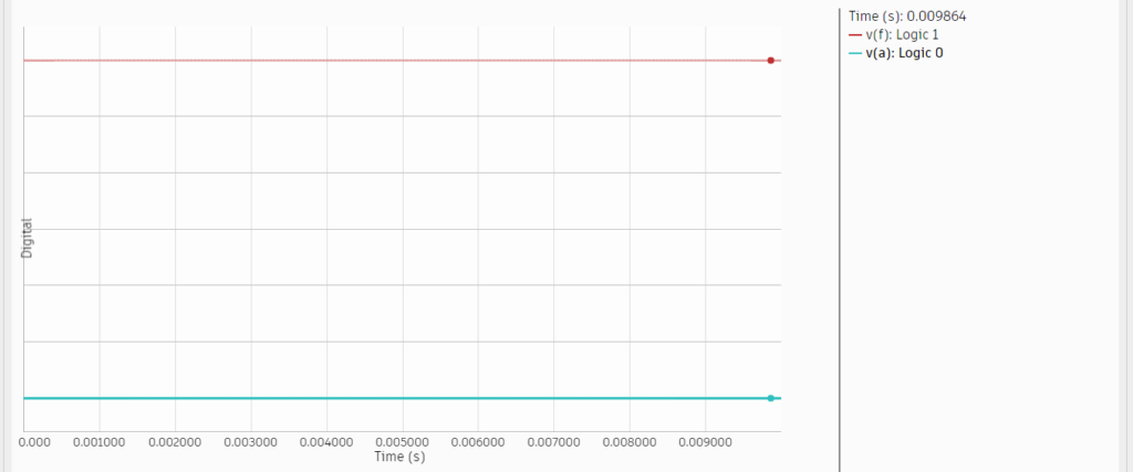
The blue line represents the input signal, which is present at a logic level 0 (0 Volts), while the red line represents the output signal, which resides at logic level 1; this is precisely how a NOT gate works. If logic level ‘1’ is present at the input, the output would be ‘0’.
Simple NOT Gate Circuit
Let’s see how we can use this gate to implement a practical circuit used in real-life applications. Consider a cabinet where you wish to install a bulb that lights up when the cabinet door is opened and lights off when the door is shut. To do so, you will need a pushbutton switch installed inside the cabinet, such that, when the door closes, the pushbutton remains pressed, and when the door is opened, the button goes back to its original state; where it is not pressed.
We can simulate this scenario by using a digital pulse signal representing the door’s opening and closing. When the door is open, the button is not pressed; hence it is characterized by a logic level 0. The NOT gate inverts this signal into a high logic level, which in turn, switches the light on. The circuit and its simulation are illustrated below:
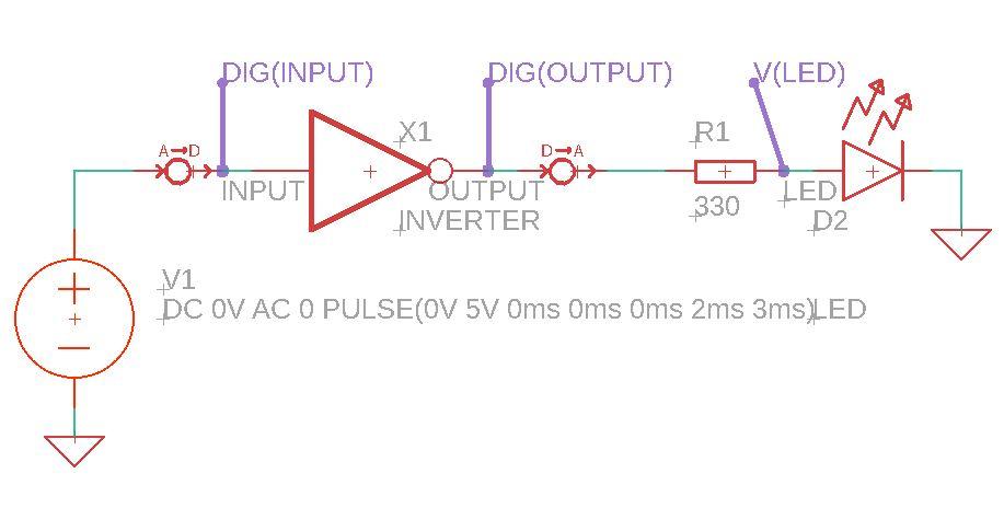
In the simulation results shown above, the blue line represents the pushbutton input, which means when the cabinet door is closed, the input is at logic level 1. The output signal (represented by green and red) is low, which means the bulb is turned off. Similarly, when the cabinet door opens, the bulb lights up.
NAND Gate
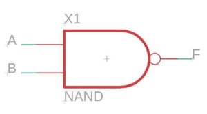
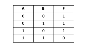
NAND gate is one of the most commonly-used logic gates. It is a combination of AND gate and NOT gate. If you look at the symbol, it is merely an AND gate with a tiny ‘bubble’ connected in series with it; this bubble represents the inverter, i.e., NOT gate. The operation of the NAND gate is similar to AND except that the output is inverted. For instance, if you have two ‘high’ signals and perform the AND operation on them, you will get a high output. But with NAND, you will get a low output for two 1’s at the input terminals. Thus, we can represent the NAND gate with the following Boolean equation:
F= A.B
Which generates the following truth table showing the output, F, for all possible input combinations:
Internal Working
Like the previously discussed gates, we can represent the NAND gate’s internal working using transistors and resistors, as shown in the circuit diagram below. Two transistors are connected in series, with the emitter the first one connected to the second transistor’s collector. The two transistors’ bases act as input terminals of the NAND gate, while the output is measured from the first transistor’s collector. For the output to be high, either one of the transistors must be cut off. We can verify the results through the simulation graph shown below.
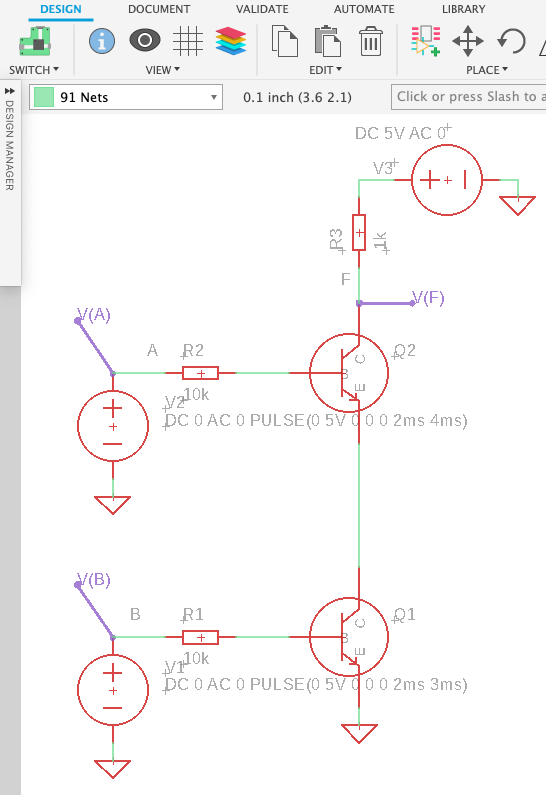
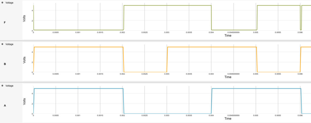
The output of the NAND gate is low only when both inputs are high. This can be seen from the simulation results above, where the red line indicates the output pulse while the blue and green pulses represent the input signals.
Simple NAND Gate Circuit
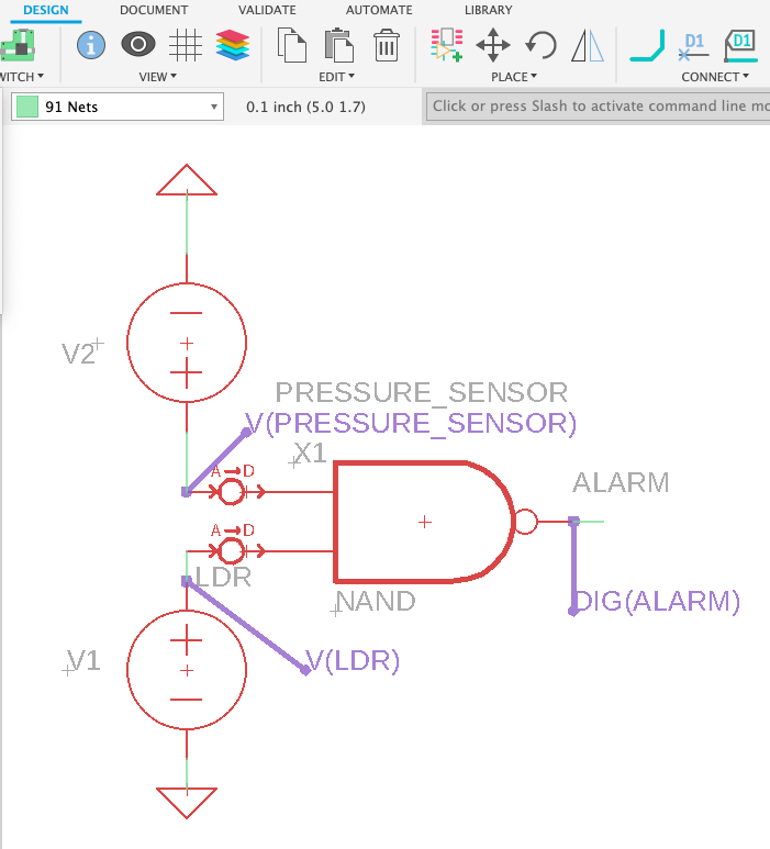
Now that you know how a NAND gate works, let’s design a simple circuit where a NAND gate performs a real-life task. You can use a NAND gate to build a simple burglar alarm that goes off when either the burglar’s shadow is detected, or the burglar stands on the pressure sensor present at the house entrance, or if both conditions are met simultaneously.
An LDR is used to detect the burglar’s shadow, while a pressure sensor is used to detect the thief’s presence through the pressure that their body exerts on the ground. To simulate this scenario, the voltage sources are used to represent the LDR and the pressure sensor. The LDR and pressure sensor both produce a low output when the burglar is present. The simulation results are as follows:
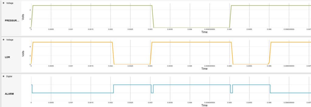
The blue pulse represents the alarm’s voltage levels, showing that the alarm is only off when neither there is a shadow present at the entrance nor any pressure sensed. This is the case when no one is present at the door of the house.
Multiple Gate Design
Using a single NAND gate to build a circuit was pretty easy, so let’s move on to designing a circuit with multiple NAND gates. We can use various 2-input NAND gates to design a 4-input NAND gate. When all four inputs are high, the output will be low, and when either one of the inputs is 0, the outcome will be high. Two NAND gates are used as input gates. Then two intermediate NAND gates are present, which sends the signal to the output gate. A total of five NAND gates are used to design a 4-input NAND gate, as shown in the circuit below.
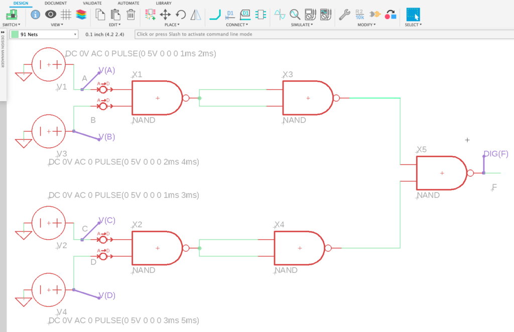
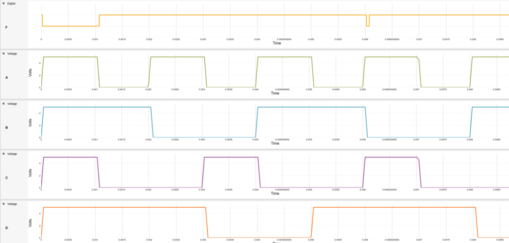
The red pulse shows the output (F) of the 4-input NAND gate circuit, which is low only when all four inputs (A, B, C, D) are high. Otherwise, the output remains high.
XOR Gate
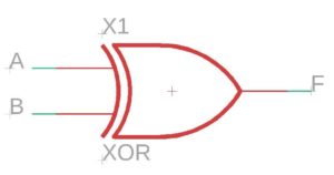
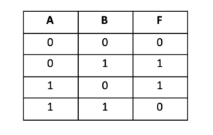
XOR gate, also known as the Exclusive OR gate, is widely used in many logic and combinational circuits. The output of this gate is high only when both of its inputs are different with respect to each other. i.e., if the input signal is either “01” or “10,” only then the output would be “1.” Otherwise, the output will be low, i.e., logic level 0.
Alternatively, we can understand the working principle of the XOR gate in another way. Its output is high when there is an odd number of 1s present at the input terminals. For instance, if we have the inputs as A=1 and B=0, then we have only one 1, i.e., an odd number of 1s present at the input, so the output will be high, i.e., F=1. The Boolean expression for a 2-input XOR gate is written as:
F=AB+AB
Which generates the following truth table:
Internal Working
We can understand the XOR gate’s internal working using a combination of other logic gates such as OR, AND, and NAND. Remember that the XOR gate is not an original gate, it is a combination of basic gates that we have studied earlier.
Before moving on to the circuit, it is essential to understand that there are different ways to write Boolean equations. You can simplify an equation and change it into another form by applying simple Boolean algebra rules. We won’t go into the details of the mathematics involved here, but all you need to know at this stage is that we can also write the Boolean equation for a 2-input XOR gate as follows:
F=A+B.(A.B)
Now let’s move on to the XOR equivalent circuit.
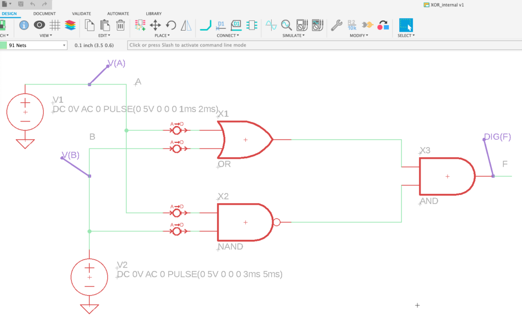
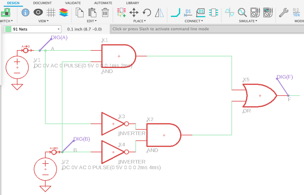
As you can see, the inputs A and B are applied to the OR and NAND gates, and then their outputs are connected to the inputs of an AND gate. The outcome is exactly what we get using an XOR gate.
If you form the equation for the output F, the gates’ equations will match the OR gate equation. The equation for the output of the OR gate is A+B and for NAND is (A.B), and if we put these equations in the AND gate equation, we will get F=A+B.(A.B).
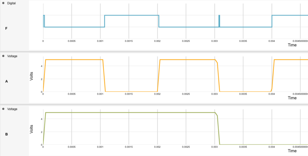
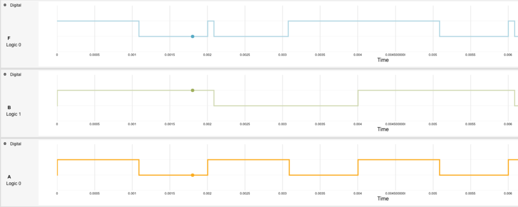
From the simulation results, it can be determined that the output is high whenever the inputs are not identical, i.e., when the input is either A=0 and B=1 or A=1 and B=0.
Simple XOR Gate Circuit
We can build a half-adder using an XOR gate and an AND gate. This circuit adds two bits at a time and generates two output bits; one is called the “sum,” and the other one is called “carry.” It is analogous to manually adding large numbers in decimal format, where we carry numbers greater than 9 on the number to the left, and then add it. The following circuit is what a half-adder looks like:
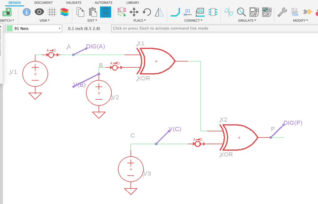
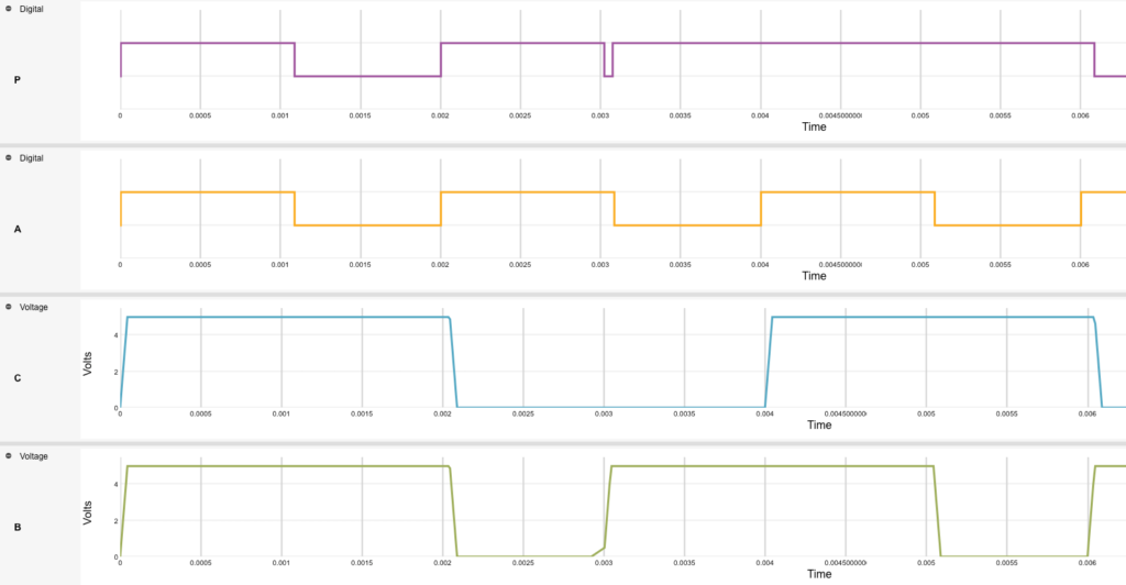
The output of this circuit is simulated as follows:
To understand this better, let’s study the truth table for a half-adder.
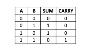
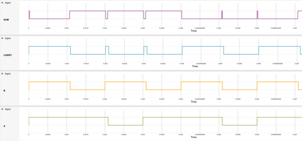
When we add 1 and 0, the sum is 1, and the carry bit is 0. However, when two 1s are added together, the sum is 0, and the carry bit is 1. This is exactly what is happening in the half adder circuit, and you can confirm that by studying the simulation graph where the red pulse represents the sum while the green pulse represents the carry bit.
Multiple Gate Design
How about using multiple XOR gates in the same circuit? An even parity bit generator for a 3-bit message can be made by using various XOR gates in the same circuit. A parity generator is a type of error-correction tool used in digital circuits. An even parity generator will first scan the message for the number of 1s. If they are even, there is no need to add a 1; hence it will add a 0 as a parity bit. Otherwise, if the number of 1s is odd, then the parity generator will add a “1” as a parity bit to make the number of 1s even. Here is what the circuit looks like.
In the simulation results, it is evident that the parity bit is 1 when the input has an odd (either 1 or 3) number of 1s, and it is 0 when the number of 1s in the input signal is even (2).
XNOR Gate
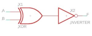
XNOR gate, also known as Exclusive NOR gate, is a part of many digital electronic circuits. Its symbol is the same ad XOR, except that there is an inverter “bubble” present at the output, which implies that XNOR’s output is opposite to that of the XOR gate. We can also represent the XNOR gate as an XOR gate in series with an inverter, as shown below.
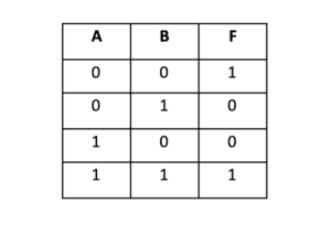
The XNOR gate’s output becomes 1 when both of its inputs are the same for each other, i.e. for a 2-input XNOR gate, the output will be high for input combinations “00” and “11.” Otherwise, when the inputs are different concerning each other, the output is low.
Since this gate produces a high output when its inputs are the same, it is also called as an “equivalence gate,” because you can detect if two inputs are logically equal or not. Another way to understand an XNOR gate’s working is to produce a high output when the number of 1s at the input terminals is even. For instance, if the input combination for a 3-input XNOR gate is “101,” then the output would be high (1) because there are two 1’s present at the input terminals, which is an even count. The Boolean equation for the XNOR gate is written as:
F=A.B+A.B
Which generates the following truth table for a two-input XNOR gate:
Internal Working
We can understand an XNOR gate’s internal working by breaking it down into a combination of the basic gates such as AND, OR, and NOT gates. Using the Boolean equation, we can design the simple logic gates circuit as follows:
The simulation results show a blue-colored output pulse, which is high only when both the inputs are logically equal. Otherwise, the output resides at logic level 0. XNOR gates are widely used in digital electronic circuits, including full-adders, subtractors, and parity checkers and generators.
Building Complex Circuits Using Logic Gates
Now that you have studied the different types of logic gates, their equations, truth tables, internal working, circuits, and applications, let’s see how we can combine all or some of the seven types of logic gates in a single circuit.
4-Bit Comparator
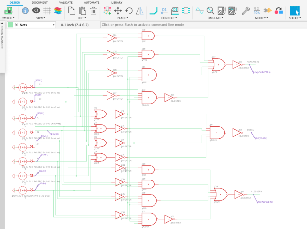
A 4-bit comparator, as the name suggests, compares two 4-bit signals and generates the result as either equal to (A=B), lesser than (A<B), or greater than (A>B). It uses a combination of different logic gates to compare the four bits one-by-one. The first bit of the first word is compared with the first bit of the second word, and so on.
Consider the first 4-bit word A = A3A2A1A0 and the second word B = B3B2B1B0, where A3 and B3 are the most significant bits, while A0 and B0 are the least significant bits. A 4-bit comparator circuit for comparing the words A and B is shown below.
The input signals for the 8 bits are in the form of digital pulses that periodically swing between logic levels 0 and 1. The output is generated based on comparing the two 4-bit words formed as a combination of the 8 bits. The results are simulated below:
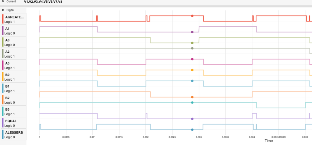
Here, the bold red line represents the A=B output terminal. At the point shown, the words A and B are equal; hence the v(equal) pulse is high. If you look at the bits’ values carefully, you will see that A0=B0, A1=B1, A2=B2, and A3=B3.
3×8 Decoder
Another complex circuit example which uses several logic gates in the same circuit is a 3×8 decoder. It has three input lines (A, B, C) and eight output lines (Y0, Y1…, Y7). An enable (EN) pin activates the output based on the input combination. Each output is activated via a 3-bit input code that is unique for each output.
Using a combination of AND & NOT gates, we can build the circuit as follows:
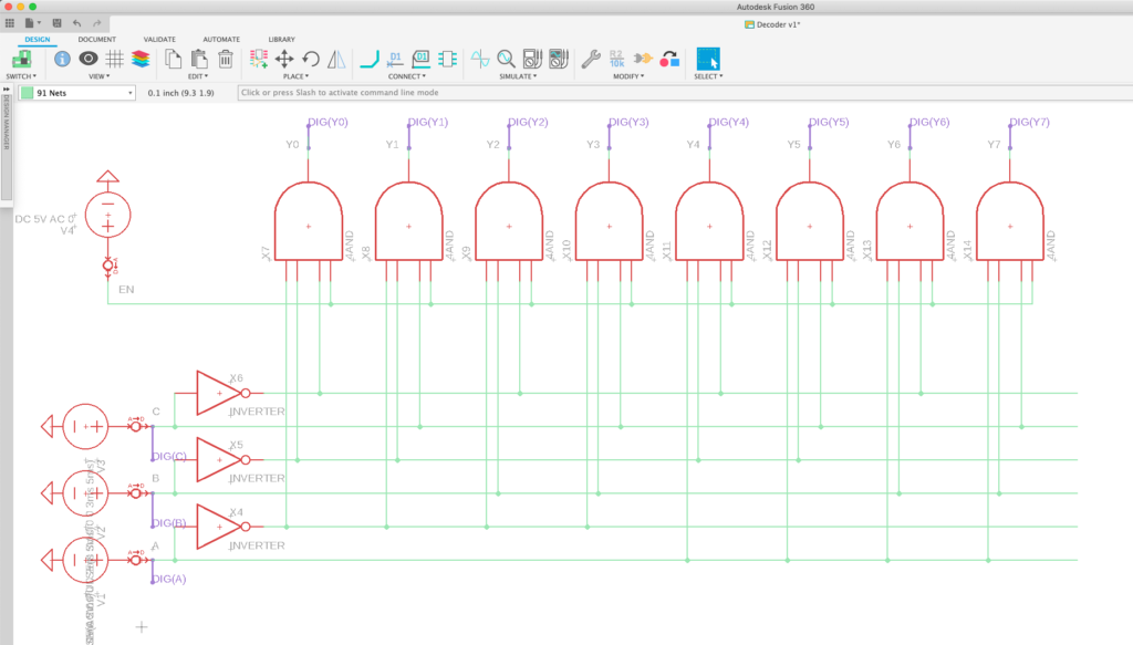
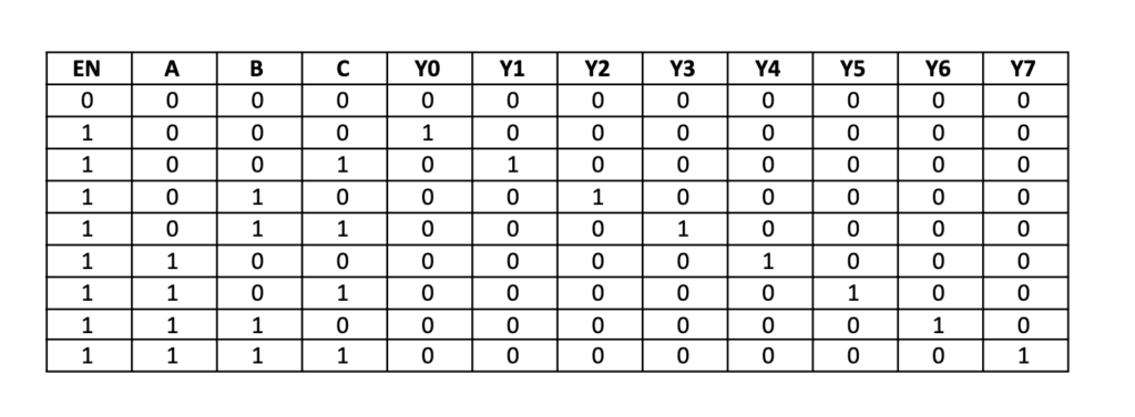
Eight AND gates produce the outputs Y0, Y1, Y2, Y3, Y4, Y5, Y6, and Y7, while the NOT gates are supplied with the inputs A, B, and C. The outputs vary according to the table below:
This can be verified through the simulation results shown below:
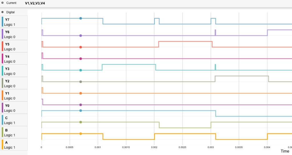
The output waveforms vary according to the truth table shown above. For instance, when all three input signals v(a), v(b), and v(c) are high, the output Y7 is activated, as shown in the simulation results.
Logic gates are beneficial electronic components because they can perform many tasks, including mathematical operations and conditional programming. They are widely used in microcontrollers, microprocessors, and several other electronic devices present around you. All you need to know is how they work, and you can construct digital logic circuits all by yourself and check their results through EAGLE simulations.
Are you ready to test out these exercises yourself? Fusion 360 gives you access to comprehensive electronics and PCB design tools in one product development platform—try it today!
![]()