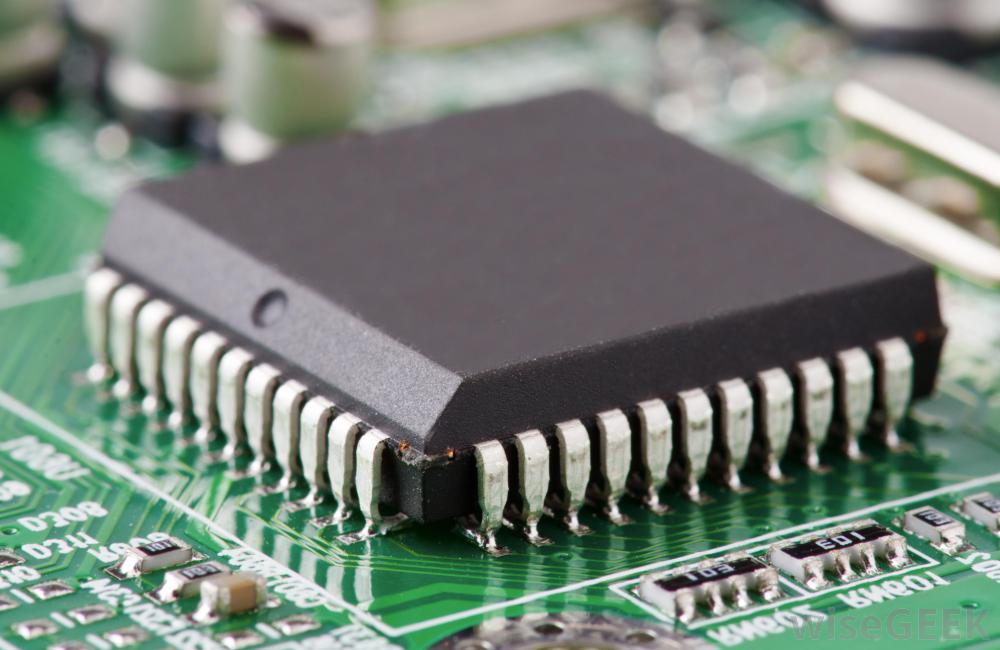
It’s that little mastermind behind all of our electronics, plotting its way to take over the world. No, we’re not talking about Pinky and the Brain here, but the integrated circuit, or IC! These little black chips are filled with much mystery, but what kind of powers do they hold?
The main ingredient of today’s electronics rests on the hidden power of the integrated circuit, and you’ll likely be using them in your own projects. So here’s everything you need to know, and Moore, on how an IC works.
What is an integrated circuit?
So, what exactly is an integrated circuit? In its most basic form, an integrated circuit is simply a collection of teeny tiny electronic components organized on a piece of silicon. Compared to their larger brothers and sisters, the components found on an IC can be nearly microscopic in size. Each IC contains a unique collection of diodes, transistors, microprocessors, capacitors, etc… all found on something smaller than a dime!

What’s the benefit of putting all of these components together into one integrated circuit? There are many! Here are just a few:
1. Space Savers
Instead of requiring an entire printed circuit board filled with a ton of transistors, diodes, and other parts, you can get all of that advanced functionality in a fraction of the size.
2. Greater Complexity
The level of complexity found in such a small package has allowed us to build some pretty amazing things. Like self-landing rockets and satellites with built-in navigation. Imagine trying to make those things with billions of through-hole components!
3. Common Goals
By creating a tiny integrated circuit with an exact purpose, you can put a bunch of these together to achieve a common goal. Need a tracking device for your car? One IC can provide GPS, another can send messages, and a final microcontroller IC can control all the data going back and forth.
And, of course, you also have the benefit of taking all of those separate yet connected parts found on a conventional circuit and putting them all together in one place! That gives you the advanced functionality you need in a pre-made circuit without having to build it yourself.
The integrated circuit truly is the brains behind all of today’s electronic devices, and you’ll be hard-pressed to not find them everywhere, like in radars, televisions, video processing, missiles, and yes, even juice makers! The list is endless. Just take a quick scan of all the electronic devices in your home, and you’re bound to find an IC inside nearly all of them. But from where did they come?
The beginnings of the integrated circuit
Before the integrated circuit rolled around, vacuum tubes were the kings of the day, being used to amplify electrical signals and power computers the size of an entire room! But these monolithic vacuum tubes broke down regularly and pumped out a ton of heat in the process.
So in 1947, three American physicists one-upped the vacuum tube by making the first transistor. These things were a fraction of the size of a vacuum tube, used way less power, and didn’t break nearly as much. And if you combine a bunch of these transistors together? You get an integrated circuit!

The first integrated circuit
The first integrated circuit was developed by two gentlemen — Jack Kilby and Robert Noyce. Kilby was working at Texas Instruments at the time, where he had an idea to construct all of the parts of an electronic circuit on a single chip. He soon put his idea into reality, and built the world’s first integrated circuit on September 12, 1958, on a slab of germanium.

Over at Fairchild Semiconductor, Robert Noyce was also working away. Using a new chemical technique known as the planar process, Noyce went on to create another variation of the integration in 1959; this time put to work on silicon, which is still used today!

Of course, both companies rushed to secure a patent on their inventions, and on April 25, 1961, the patent office awarded the first integrated circuit patent to Robert Noyce. Today, both Kilby and Noyce are credited with inventing the integrated circuit. Kilby later received the Nobel Prize in Physics in 2000 for his contribution to the future of electronics. The world would soon move past the simple one-transistor integrated circuit from Noyce and Kilby, and an entire manufacturing process would soon be born to pump out these little black chips to the world.
How an IC Is Made
At the heart of an integrated circuit are layers of silicon wafers (semiconductors) and copper that come together to create the electronic components that we use today in our breadboards – transistors, resistors, diodes, etc. in a miniaturized form. When you organize all of these parts together in an integrated circuit, then you have created a die. But how exactly is this die made? That’s where doping comes in
Semiconductors & doping
Semiconductors are not just conductors or insulators; they’re both! While many people thought that conductors and insulators were evenly split categories, this truth gets a little fuzzy the farther you journey into the periodic table. There are several materials, including silicon and germanium, that can act as both insulators and conductors depending on what kind of impurities are added to them. This process of adding impurities is called doping. Here’s how it works in a nutshell:
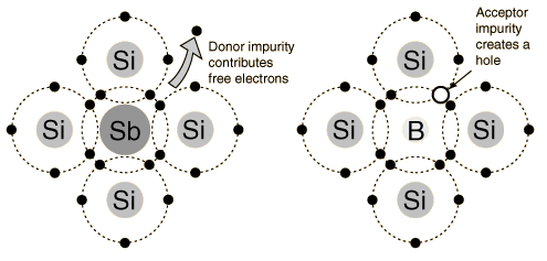
- N-Type Doping: Let’s say you have a piece of silicon, and you add the chemical element antimony to it. This is going to give silicon more electrons than it normally has, while also allowing it to conduct electricity. This doped silicon is called N-type silicon.
- P-Type Doping: If you take the same silicon and add the chemical element boron to it, then you’ll remove some of the silicon’s electrons, leaving behind gaps that act as negative electrons that can carry electric current in the opposite direction of n-type silicon, and so you’ve created p-type silicon.
- Putting It Together: By placing both n-type and p-type silicon together, you can create pathways for electrons to flow. And this exchange of electrons being exchanged is the basis behind the on and off, or 1 and 0 binary function of today’s transistors, integrated circuits, and digital electronics!

Doping methods
There are several methods to make the doping process happen. One of them is called sputtering, which is basically where doping material is fired at a silicon wafer in machine gun-like fashion. There’s also another method called vapor deposition, which uses gas to transmit the impurities as a film onto the surface of a silicon wafer. Here’s the entire process that a piece of silicon will go through to become an integrated circuit:
1. Wafers
Scientists first grow silicon crystals in the shape of long cylinders like a tube of cookie dough. These then get sliced super thin, creating what are called wafers.
2. Masking
Next, heat and ultraviolet light are applied to each wafer, leaving behind a coating of silicon dioxide and a protective layer called photoresist.
3. Etching
It’s now time for a chemical bath where these masked wafers will have some of their photoresist removed, leaving a pattern for where n-type and p-type areas will be placed.
4. Doping
The etched wafers are heated yet again with gasses that contain our doping impurities to create our n-type and p-type silicon.
5. Testing
The now completed wafers are now run through a testing machine to verify proper connections. Any wafer that doesn’t pass gets tossed.
6. Packaging
All of the wafers that pass the testing phase are then packaged into the black boxes that we’re used to seeing on a circuit board!

Common types of ICs
Integrated circuits come in all shapes and sizes, and can all be wrapped up into three general categories:
1. Digital Integrated Circuits
These ICs work on the binary system that powers all of the digital electronics of today, using a system of 1s and 0s to make some amazing things happen. In digital integrated circuits, you’ll find logic gates, transistors, etc.. all bundled into a single chip to power things like an Arduino or Raspberry Pi.
2. Analog Integrated Circuits
Unlike its digital cousin, the analog IC works by tackling those always-changing analog signals and can perform some heavy tasks including filtering, amplification, and modulation.
3. Mixed-Signal Integrated Circuits
When you combine both digital and analog functionality on a single chip, then you’ve created a Mixed-Signal IC. You’ll find these guys being used for things like clocking/timing regulation and digital-to-analog or analog-to-digital conversion.
Within the realm of digital integrated circuits, you’ll find a ton of variety, including logic gates, timers, microcontrollers, microprocessors, FPGAs, and sensors. These ICs all pack in millions and even billions of transistors on a single circuit. But how do you tell the difference between each? This is where package types can help.
Making sense of package types
The brain of an integrated circuit is skillfully hidden beneath a protective package that you’re used to seeing on a circuit board. Package types are all standardized, making it easy to solder to circuit boards or connect to breadboards for prototyping. On each package, there’s a set of silver pins, and these allow the IC to connect to other parts of your circuit. While there are many different package types, we’ll cover the most common that you’re bound to encounter in your projects:
Dual-inline packages (DIP)
This package type is part of the through-hole family, and you can easily recognize these chips by looking for their long, rectangular shapes with parallel rows of pins. This package type is ideal for use on breadboards and can include anywhere from 4 to 64 pins.

Small Outline Packages (SOP)
SOP ICs are closely related to DIPs, except they’re applied as surface-mount components instead of through-hole. These chips won’t be used in your breadboarding experiments and will require some advanced machinery to apply precisely. SOP ICs come in several varieties, including Thin Small-Outline Packages (TSOP) and Thin-Shrink Small-Outline Packages (TSSOP).

Quad flat packages (QFP)
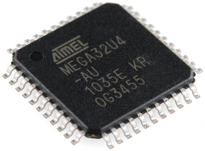
This package type is easily identified by pins jutting out from all four directions of the IC. These useful chips can have anywhere from 8 to 70 pins on each side, which can give them a whopping 300 pins to work with during a PCB layout process! You’ll find a ton of microprocessors using the QFP package type, including the popular ATmega328.

Ball grid arrays (BGA)
The last package type, and also the most advanced is the Ball Grid Array. These complex package types include small balls of solder on the bottom arranged in a pattern or grid. Routing all of the pins on a BGA can be quite difficult, often taking hours to route the nets out of the tight spacing (called fanout routing). You’ll find the BGA package type used for only the most advanced microprocessors, like those on the Raspberry Pi.

Moore’s Law and the future of integrated circuits
Since integrated circuits came into existence in the 1960s, engineers began putting dozens of components on a single chip in what was called small-scale integration, or SSI. Shortly after, hundreds of components were being placed in the same footprint, then thousands, and millions! Noticing a trend here?
Gordon Moore, co-founder of Intel, sure did. Moore made the observation, and also the prediction that the number of components being placed on a chip was doubling roughly every one to two years, and would continue to do so. This is the famous Moore’s Law.

Today, Moore’s Law is running into some trouble. By 2006, we were squeezing in over 300 million transistors on a single chip. But today’s ICs are “only” packing in about 1 billion transistors. This is way off of Moore’s prediction, which says we should be using 4-5 billion. So what’s the problem? Several things:
1. The problem with space
The more components that we pack into the same space, the more problems we find. Like possibly having one rogue atom go astray that can ruin an entire chip and provide some questionable reliability.
2. It keeps getting hotter
Having millions and billions of transistors packed into such a small space creates a huge problem with heat, how are you going to handle that increase in temperature in the already shrinking size of our devices?
3. Strange behavior
When you start packing in transistors together, then quantum mechanics come about, and electrons start jumping around for no reason. This becomes a problem in your computer, where stray electrons can mean the difference between clean and corrupted data.
So what’s the solution? Some propose that it’s time to end our use of silicon and move on to other conductive materials like graphene. But we still haven’t figured out how to reliably manufacture this new material. There’s also the option to replace electrons with something faster, like photons! Whether either of these alternatives will power the future of our computers is yet to be seen.
Here’s a great video that sums up the challenges we’re facing with Moore’s Law, and where we might be headed in the future (laser computers, anyone?)
Today, electronics. Tomorrow, the world!
So that’s it for the wild and crazy world of integrated circuits. Can we guess what the future will hold as we advance into packing more and more transistors into a smaller space? It’s anybody’s guess. But if there’s one thing for certain, it’s that integrated circuits will continue to serve as the little masterminds behind all of our electronic devices.
We’ve seen just how useful these things can be, providing the brains behind things like radar, televisions, video processing, and our very own computers. And with a ton of different package types to work with, you’re bound to run into your very own IC when you start your first electronics project.
Ready to get started on your first electronics project today? Try Autodesk Fusion Electronics today.