
V2.0.7421 – January 29, 2020
We made some important fixes in this update:
• We improved overall stability around new Electronics Design workflows and fixed some crashing issues when some of you tried to close Fusion 360.
• Commands that belonged to 3rd party add-ins, which were added into workspaces other than the Design workspace appeared to be greyed out and unavailable. Now they are available again.
• Some of you were experiencing crash issues when trying to fix broken assemblies.
• grazianoZ8TY8 found that “Find in Browser” no longer worked the way it was intended to. This made finding parts in a large assembly very difficult. Now it’s fixed.
V2.0.7402 – January 22, 2020
[toc]
[icon name=”star” class=”” unprefixed_class=””] Introducing Electronics Design in Fusion 360
The year is 2020. Humanity has come a long way since the days of the drawing schematics with pencil on blueprint sheets. Fusion 360 has been taking design and manufacturing by storm, integrating technologies into a cohesive and easy-to-use product development experience. Now we’re proud to introduce another major piece of technology that can help you transform the way you design your products. Hold onto your butts – it’s about to get electric.
We’ve shared with you that we’ve been working on this during our Fusion Academy event in Portland, Oregon as well as at Autodesk University 2019 in Las Vegas. As of this product update, Electronics Design workflows are now not just an integration between EAGLE and Fusion 360 – it is now directly implemented within the Fusion 360 software, and is available for you to use. Eagle users and Fusion 360 users, you are all in for a treat.
The Fusion 360 Way
Why are we doing this? Simple. It’s part of the Fusion 360 philosophy. Since the very beginning, we’ve set out on a mission to bridge the gaps in the product development lifecycle. We’ve built Fusion 360 to be the single platform that brings all the tools and disciplines closer together, enabling you to connect with your fellow industrial designers, mechanical engineers, electrical engineers, analysts, machinists, and beyond, earlier in the development stage and work with each other more as a team, less as silos.
https://medium.com/svb-inside-innovation/the-consumer-electronics-industry-isnt-dead-it-just-needs-to-adapt-its-business-model-eaee0eb4e53b
If you just look around your desk, you’ll see that many of the products you use have electronics built into them. The world is more connected than ever, and if Fusion 360 is the end-to-end product development platform, it absolutely needs to have the tools for you to design electronic circuitry.
By tightly integrating electronics design into the Fusion 360 experience, you’re now able to create, design, and manage associative circuit schematics, PCB layouts, and 3D representation of your circuit boards like never before.
Let’s Get Started
There’s a lot to cover here (picture and GIF heavy), and just like other areas in Fusion 360, there are a number of valid ways to get started, depending on what you’re starting with. To keep it simple, let’s jump in and explore how to begin from scratch, and the key things you should know right away.
1.Create a New Electronics Design
Much like a new Design document, Creating a new Electronics Design will open its own dedicated Electronics Design document tab.
Within an Electronics Design document exist 3 different types of entities, a Schematic layout and 2D PCB layout, and 3D PCB design. Creating them will appear in the browser, just like how design entities appear in the Design document. Think of this space as an overview of the entire electronics design.
Schematic
For those of you new to the electronics world, an electronics schematic is like a recipe for how a piece of electronics is built and should work. It tells you what the ingredients are how they should be used to make up the end product.
When you start a new Electronics Design, you can choose to create a new Schematic document from scratch or reference an existing Schematic.
2D PCB
The PCB (printed circuit board) document is a physical representation of the circuit board itself as well as the layout of all the packages that will eventually go on the board, in relation to the schematics defined in the schematics document. These PCB documents will also connected to the 3D PCB design, which we’ll get into later.
2.Create a New Schematic
Just like working in any other Fusion 360 workspace, the tools here are laid out in a way where you should work left to right, with 4 tabs (Design, Document, Validate, and Automate), housing all the appropriate tools you need to draw your schematic.
Within the Design tab, the Switch panel allows you to quickly switchover to the PCB document, whereas the View panel provides you a couple of tools to view additional info on the schematic as well as a visibility option (as accessible view the navigation bar at the bottom).
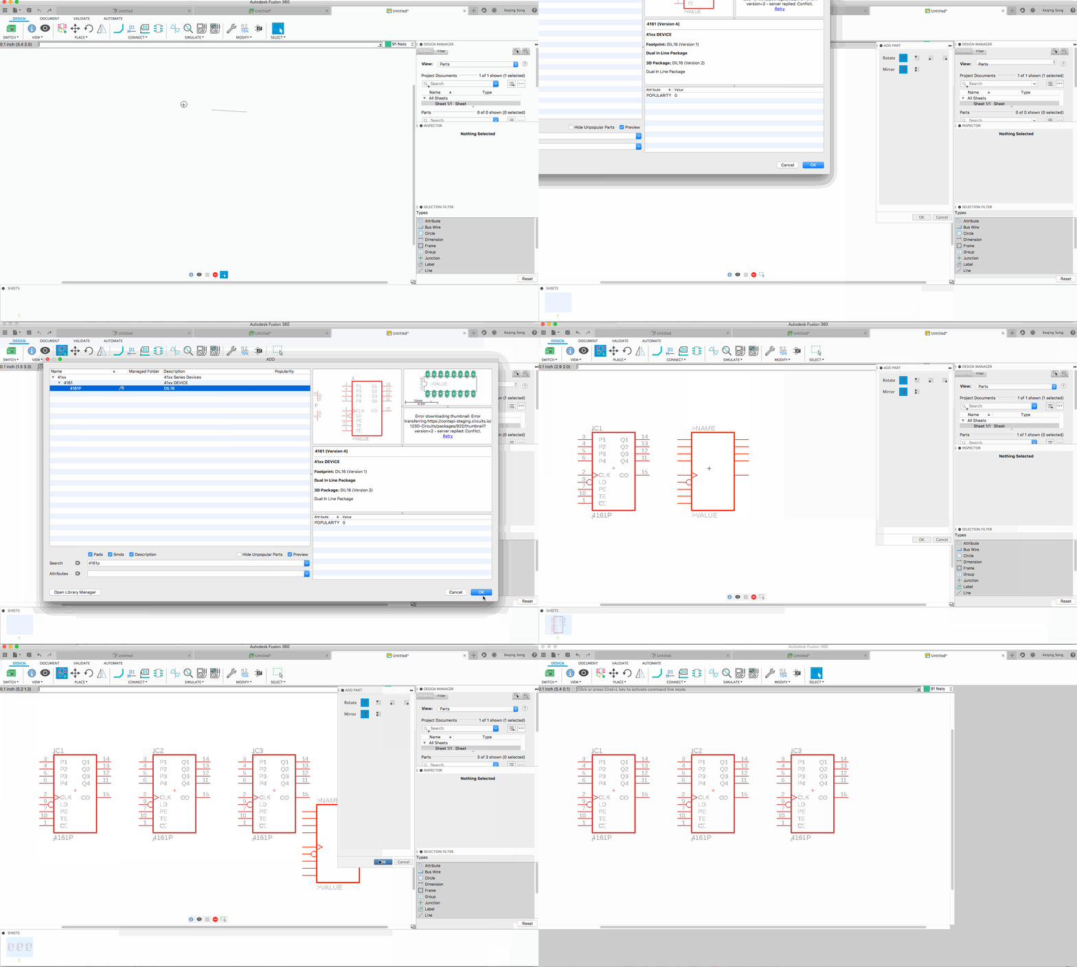
Add Part will bring you to the part library where you can browse or search through the thousands of electronics parts, each with their own schematic representation.
Once you’ve found the one (in this case, schematics for a memory chip), hit OK and the schematic will appear on your cursor, ready for you to place in canvas.
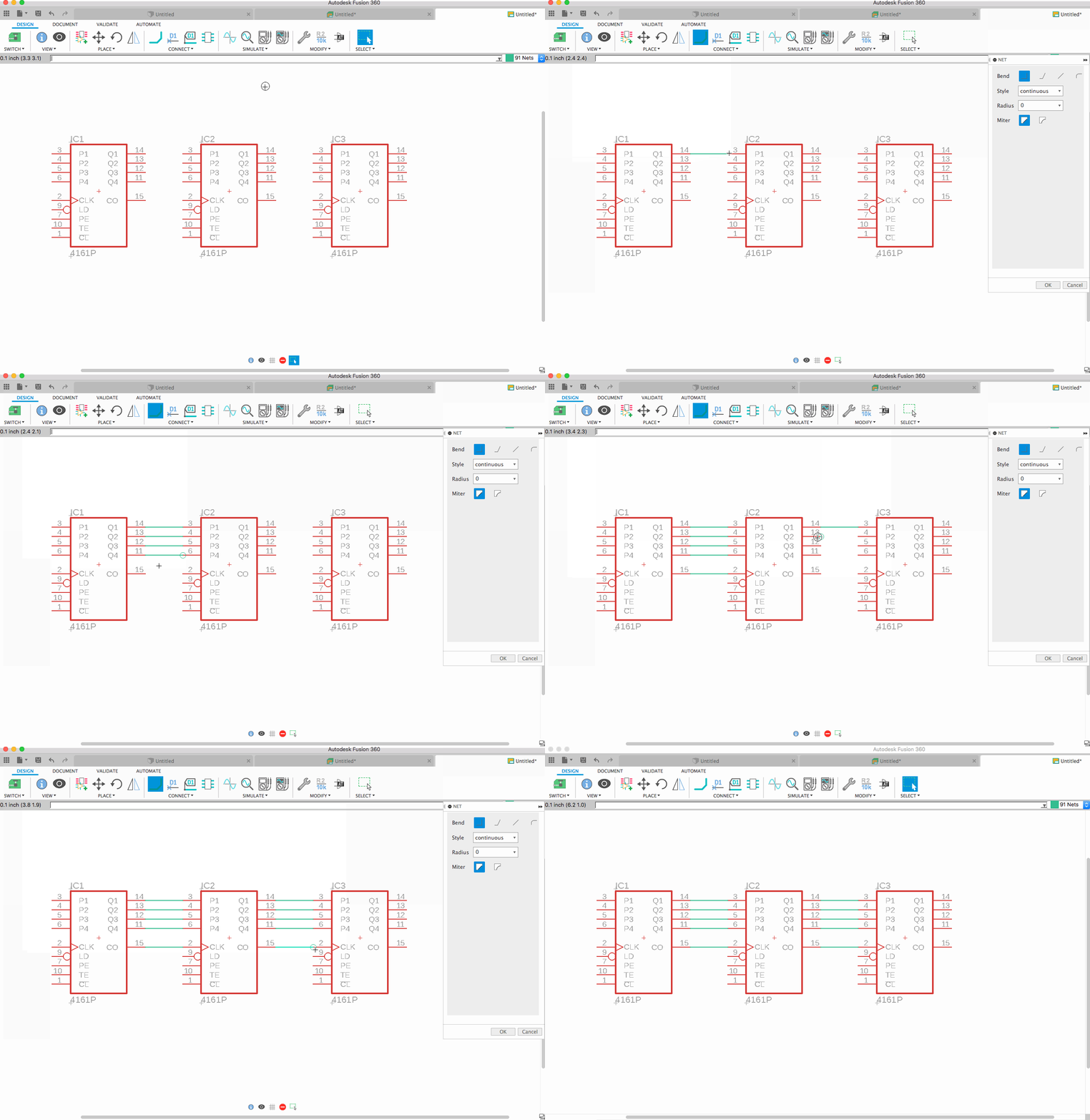
The next step is to connect the parts, and the Connect panel has a number of tools to help you do that. Since this example in particular is simple enough, you can use the Net tool and connect them one by one.
3.Create a New PCB
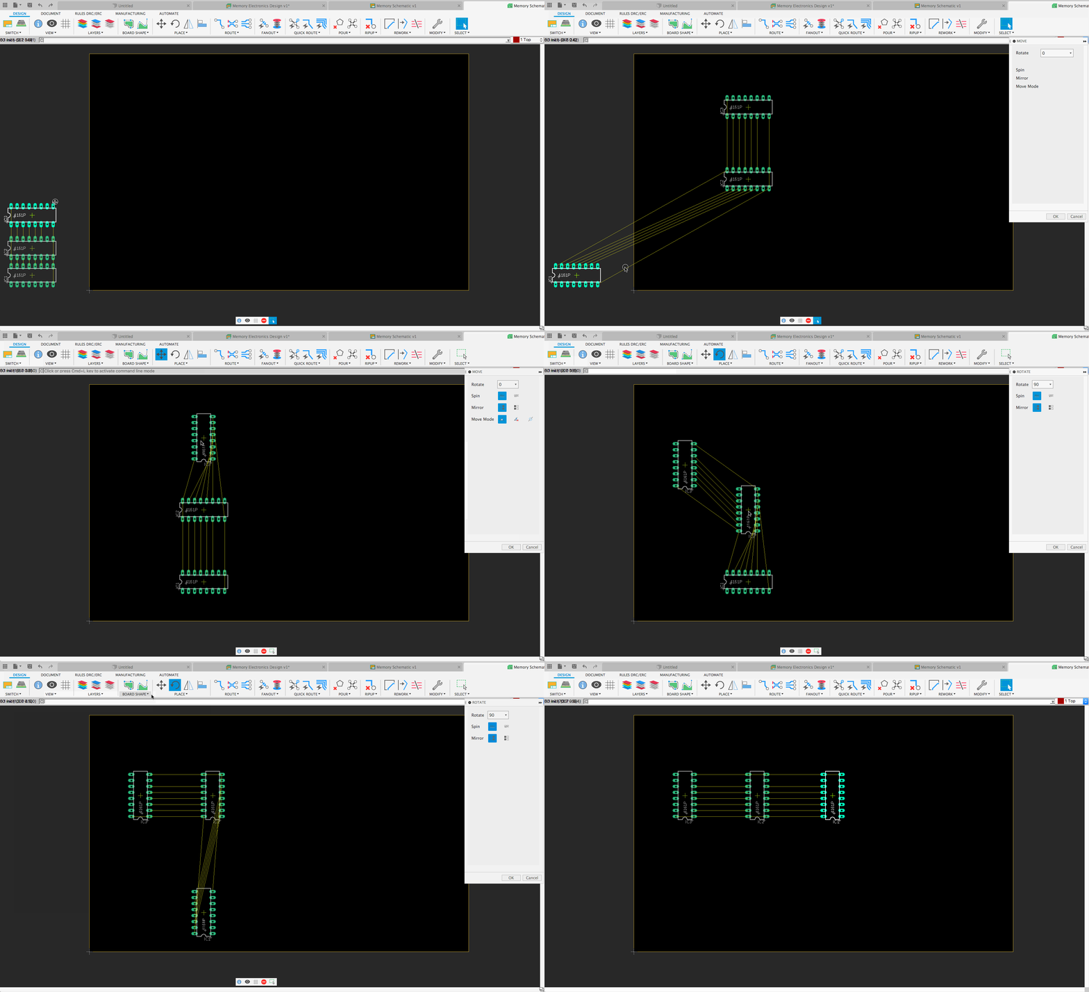
Now that you have a schematic laid out, you’re now able to create a PCB representation. Do this by clicking on the Switch to PCB document icon. This will take you to the PCB layout environment, where we can work on placing and organizing our parts. Notice that the connections are automatically represented.
4.Edit Board Shape in 2D
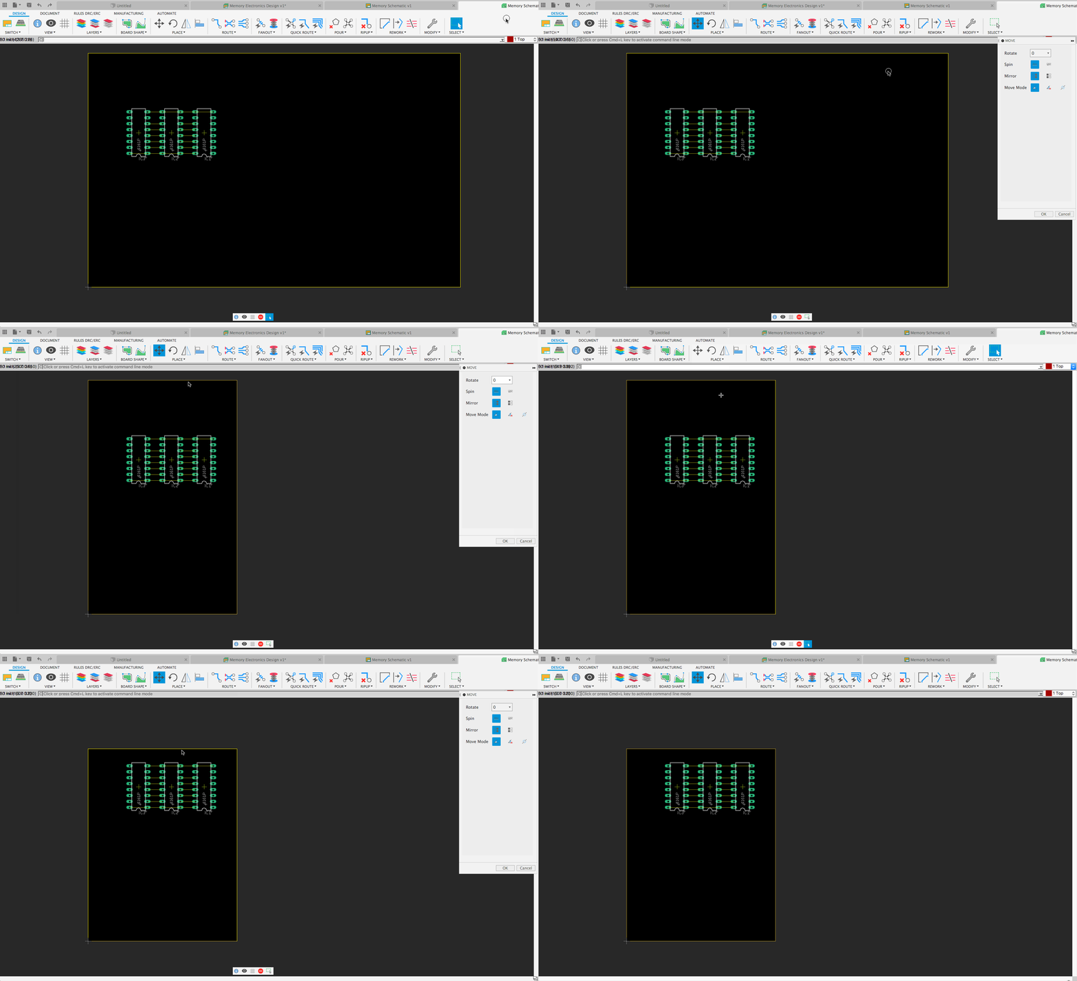
If you didn’t define a specific board shape to start with, Fusion 360 will automatically draw a default rectangle board for you as a starting point. You can also resize the board to a more appropriate size by simply dragging the outer edges.
Of course, boards are not all rectangles, and that’s why there is a panel dedicated to creating the board shape we need, tools like Outline Polyline, Spline, Arc, and Circle at our disposal. They behave just like tools in the sketching environment, and provide the flexibility you need to create custom board shapes.
You can also use the Outline Circle tool to punch holes into the board if you need one. As long as the board is shown as closed-off, an Outline Circle will open up a hole based on where you’ve placed it.
Change Package Type
Remember when we selected the part, there was a preview of what the package would be? Those green areas represent the fact that this package will have pins that go through the circuit board, meaning the board in order to make the connection. This is known a thru-hole mount package. This is also shown on the PCB document.
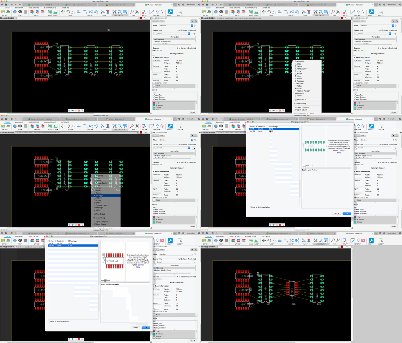
There is another type of package will there are no thru-holes; there are soldering points where the package is to be soldered on to the board, known as a surface mount package. you can select this type of package by right-clicking on the part we want to edit, pick Package, and select the solder one.
Route the Traces
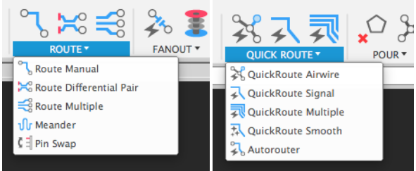
The yellow lines that connect each package indicate how they are connected, but do not represent how the connections are to be routed on the board. That’s why there are tools in the Route and Quick Route panels you can use to design how the traces are to be routed on the PCB.
After you’ve saved the 2D PCB document as well as the schematic document, your Electronics Design document will reflect both items.
5.Create 3D PCB
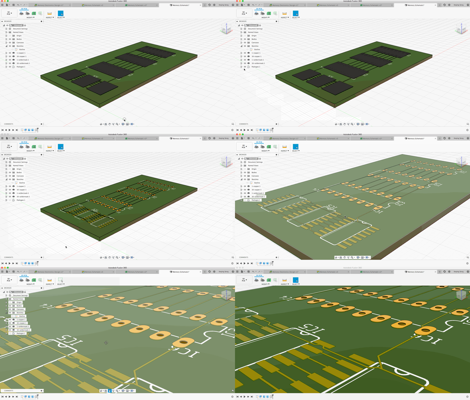
Here’s where the magic really begins to happen. Now that we have a 2D PCB layout ready to go, we can view what it’d look like as 3D PCB by clicking on the View 3D PCB icon.
Bing! Everything from the board, silk screen, copper traces, and packages are created as 3D entities in the 3D PCB environment. With familiar Fusion 360 controls, you can turn on and off the visibility of each entity.
Edit board shape in 3D
Clashes between the circuit board and how it’ll be mounted to the final product are bound to happen. Changes are inevitable. And of course, you can still update the board shape in the 3D PCB space by editing the sketch itself. The board itself is based on the 2D sketch, allowing the 3D model to be fully parametric.
Since the 3D PCB is linked to the 2D PCB layout, once the edits are done, you can push the change to the 2D PCB so that the change is reflected appropriately. This works both ways.
Toggling to the Electronics Design document will reveal the overall view of the schematic, 2D PCB, and top and bottom view of the 3D PCB.
6.Fixing Conflicts
If the board shape change is drastic, pushing the change over to the 2D PCB design will reveal areas where the devices are conflicting with the out boundaries. you can also hop over to the Rules DRC/ERC tab and do a Design Rules Check, which will reveal the problematic areas.
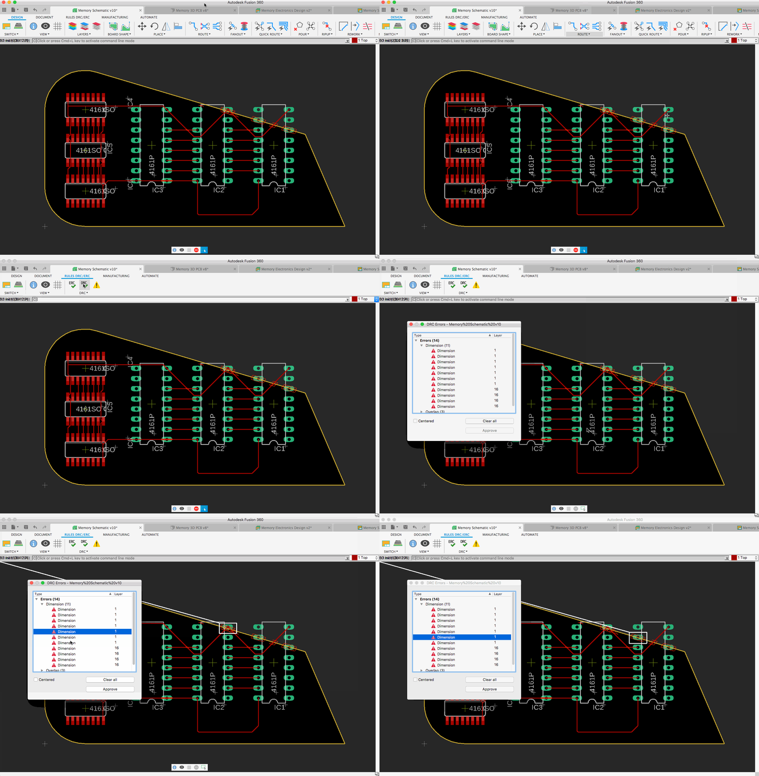
To fix this, use the Move tool to love the parts to a better spot, and then, if needed, use the Ripup tool to get rid of overlapping routes, and reroute the traces accordingly.
7.CAM Preview and Edit Colors
Hopping over to the Manufacturing tab, notice there are 3 tools in the Manufacturing panel.
CAM Preview, Processor, and Export tools will give everything you need to make the board manufacturable.
If you need the board or silkscreen to be a different color, you can change them by going to the CAM Preview tool, then click on the “gear” icon, and edit the Background, Cooper, Silkscreen, Soldermask, as well as board substrate color.
Once you’ve got your colors set, clicking on the Switch to 3D PCB will push these changes over to your 3D PCB model.
8.Create a New Electronics Library
Much like the tool library in the Manufacture workspace, it’s handy to have a library of packages that you use the most saved and ready to go. This way you don’t have to go searching in the vast sea of electronics packages. Right under New Electronics Design is the option to create a new Electronics Library.
9.Create a New Package
Once you’re in the Library document, you’ll see tools in the toolbar that lets you create your own symbols, footprints, devices, and packages.
Packages come in all different shapes and sizes. Modeling them from scratch is work no one wants to do, especially if these packages have standardized geometry. In the Fusion 360 spirit of boosting productivity, we’ve implemented a comprehensive package generator inside Fusion 360 so you can quickly search through the package type you need, specific it’s properties and dimensions, and select “Update Preview”, and voila, package created.
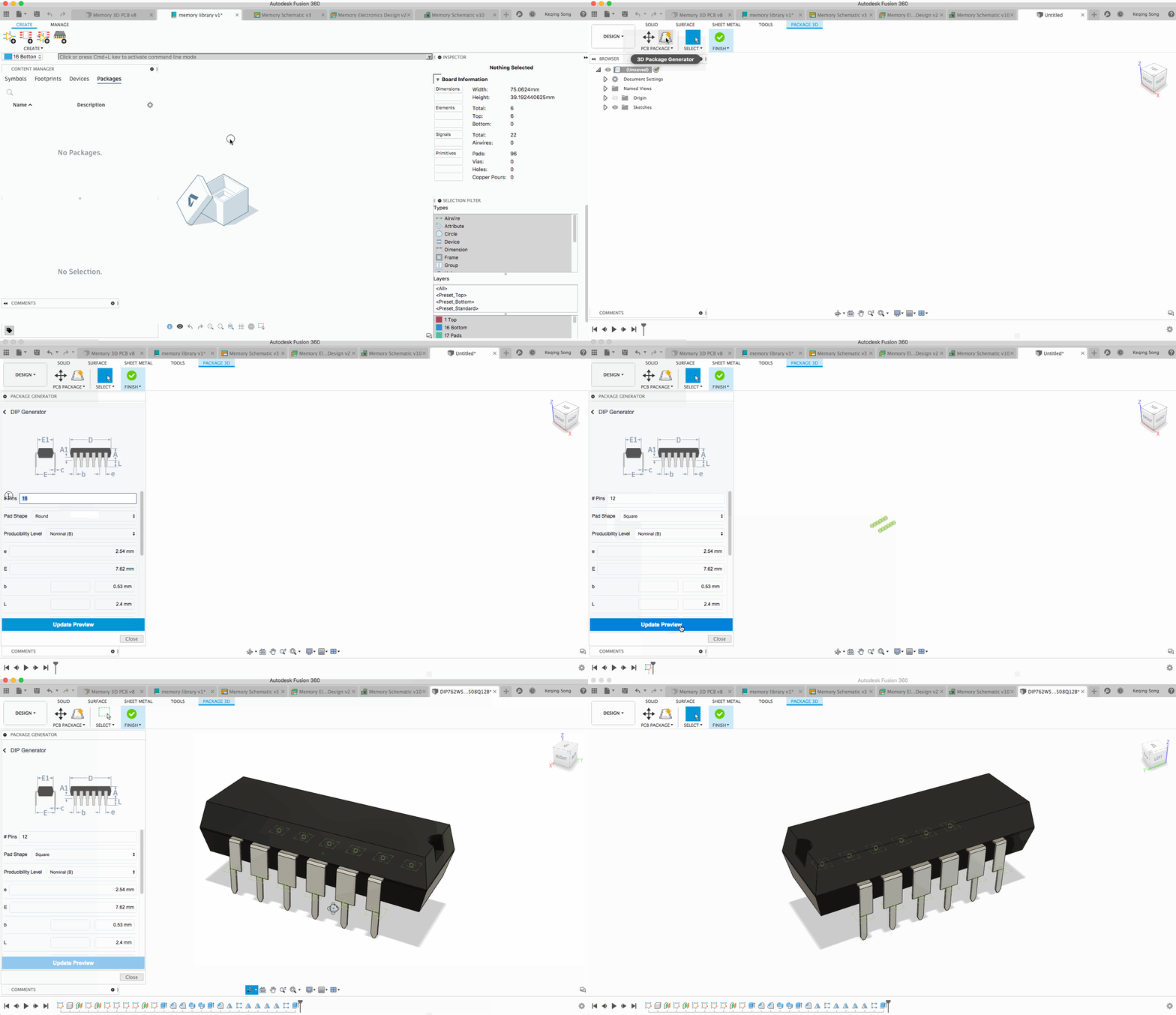
If you look closer, you’ll notice that these packages all have their own timeline history, making them fully parametric by design, that’s right, we’re not messing around here.
Once you’ve saved the package to your library, it’ll appear in the data panel project you’ve saved it to, as well as appear in the Packages tab of the Content Manager panel of your Electronics Library document.
10.Work with Multiple Windows
When you’re working with Electronics Designs, you’re inherently going to be toggling between a number of different tabs (overall view, schematic, 2D PCB, library, and 3D models). That’s why we’ve also implemented the ability for you to tear out a document tab so you can have them side by side or on a different monitor.
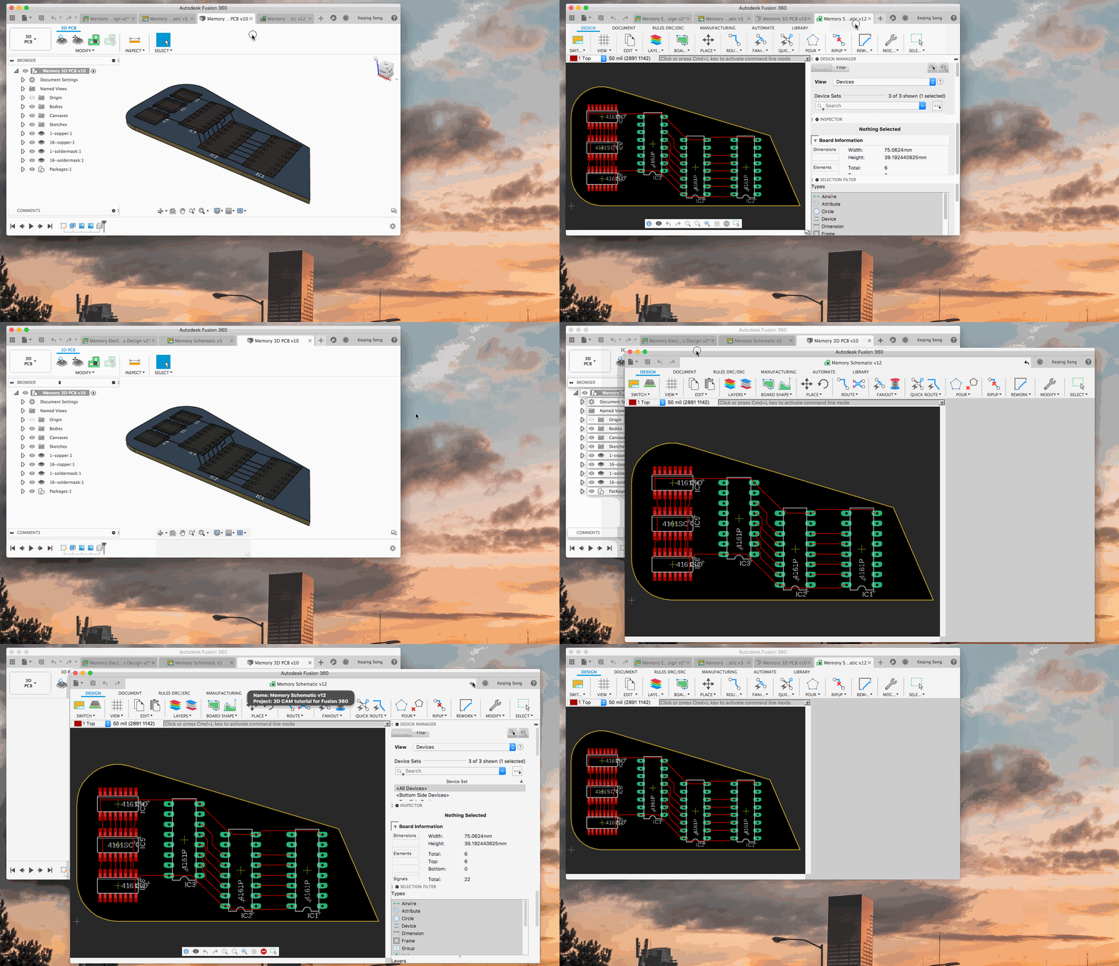
Clicking on the arrow button where the close document “X” button normally is will return the detached window back to the main Fusion 360 window.
We’ve only just begun
We just covered a lot of ground in this update post, but we’re only scratching the surface here. There is so much functionality here to explore, and we explained everything here, we could write a novel. There are other ways to begin as well, from creating a 3D PCB from a sketch profile to working with an existing 3D enclosure and defining what that PCB board should be. If you’d like to learn more, be sure to stay tuned to our YouTube channel. If you’re looking to brush-up on Electronics Design lingo, then check out our help documentation.
YouTube Channel | Help Documentation
Share your feedback
With this new functionality, we’d love to hear from you and listen to what you have to say. We’ve started a few feedback threads in our Feedback Hub, so you if have thoughts around these specific areas of the Electronics Design experience, please jump in and let us know what you think.
For feedback about the Electronics Workspace and 3D PCB Environment, view our new Electronics discussion forum.
[icon name=”lightbulb-o” class=”” unprefixed_class=””] Electronics Library Feedback Hub Thread
[icon name=”lightbulb-o” class=”” unprefixed_class=””] Schematic Workspace Feedback Hub Thread
We hope that you see the value you’re getting with each product update; it’s only going to get better and better. We’re committed to delivering next level solutions to you so you can create next level products.
Thank you and sincerely,
Keqing and the Fusion 360 Team