
Are you looking for a detailed guide to incorporating logic gates in your next electronic circuit design project? If yes, then you’re in the right place. This blog post will take you through the various types of logic gates and teach you how to use them to design your circuits the right way.
Understanding how logic gates work is one of the fundamental concepts that every circuit designer must know. They perform mathematical operations such as addition, subtraction, multiplication, and division, making it easy to design digital electronic circuits for various applications. They take two or more binary inputs, in the form of voltages, and produce an output signal, depending on the type of mathematical operation performed.
Since they work on binary inputs, there are only two voltage levels, i.e., 1 or 0. 1 corresponds to a high voltage, usually 5V, while 0 corresponds to a low level, typically 0V. The logic gate then compares these input voltages to produce a relevant output voltage again, either 0 or 1.
There are seven types of logic gates, which are listed as follows:
- AND
- OR
- NOR
- NAND
- XOR
- XNOR
- NOT
All logic gates mentioned above have two or more inputs, except the NOT gate, which has only one input terminal. Let’s look at some of the most commonly-used logic gates and see how we can incorporate them into our electronic circuit designs.
AND Gate
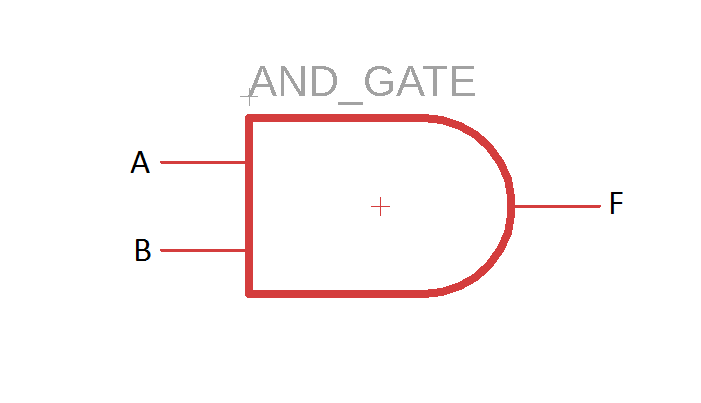
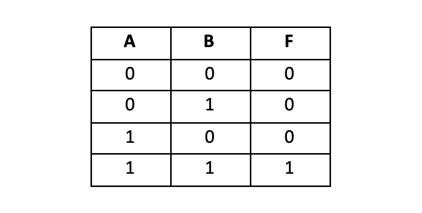
The AND gate is a very popular logic gate which works on the principle of logical multiplication. It returns a high output value only if all its inputs are high. In other words, an AND gate produces a low output voltage whenever one or more of its inputs are low. A Boolean equation for a two-input AND gate can be given as:
F = A.B
Which generates the following truth table showing the possible input combinations and their outputs:
Internal Working
The internal working of logic gates can be understood through resistor and transistor circuits. For each input, we will have a transistor connected with a resistor, forming a switch. For a AND gate, the transistors will be connected in series, and the output signal would be measured from the emitter of the second transistor via a load resistor. The diagram below demonstrates how an AND gate works.
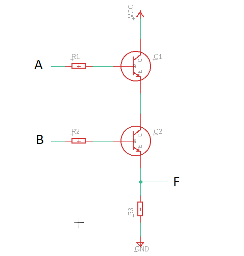
For the output “F” to be high, both transistors must produce a high signal, i.e. they must be ON. Even if one of them turns OFF, no output signal would be generated; hence, the AND gate’s output would be 0.
Simple AND Gate Circuit
Here is a simple circuit that uses an AND gate as the main processing element.
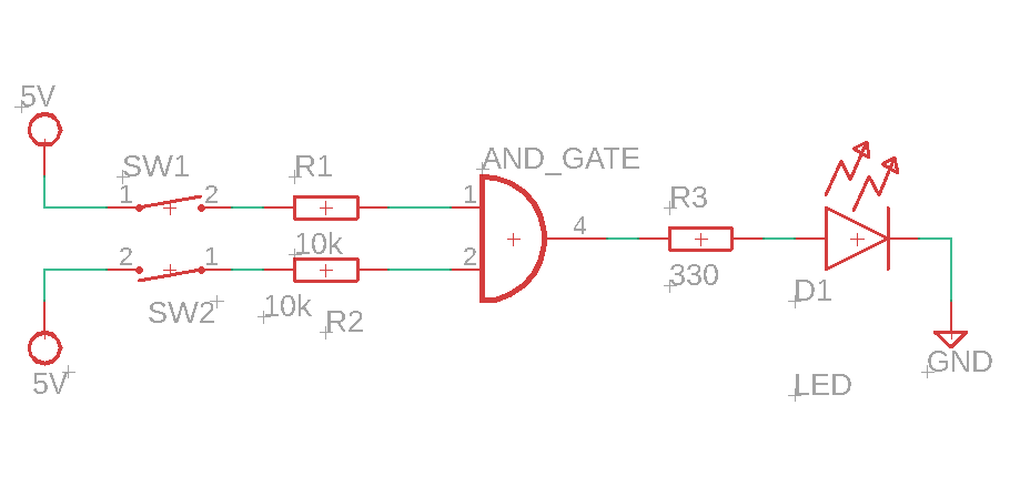
Two input signals with switches are connected to the AND gate, and an LED is connected to the output terminal, which turns on only when both inputs are high.
Multiple Gate Design
Working with one AND gate is pretty simple; let’s see how we can incorporate more than one AND gates in the same circuit.
Consider a light bulb in your room which you want to turn on when four conditions are met. Those conditions can be that the door is closed, the fan is turned on, some background music playing, and the windows are shut. If these conditions are met, they will produce a high logic level on the input terminals of the AND gate, and when all conditions are met, the bulb will light on (the output will be high). The following circuit demonstrates this scenario.
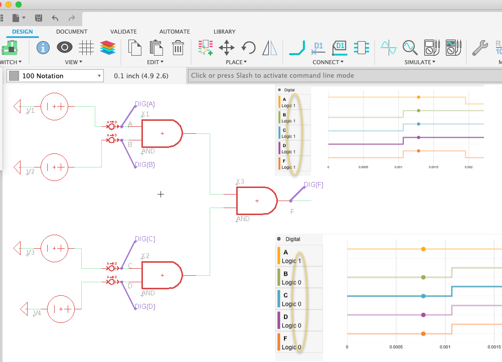
Here, two AND gates act as inputs, and one is the output gate. The four condition signals (A, B, C, D) are present at each of the input terminals of the two input gates, which produce an intermediate signal that acts as the input for the third AND gate. The final output (F) is fed to a bulb, which lights up only when all four inputs A, B, C, D, are high.
OR Gate
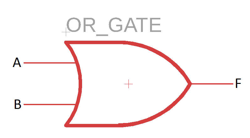
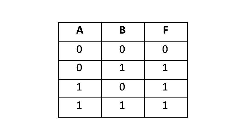
Another very commonly used logic gate is the OR gate, which performs the function of logical addition. If we consider a two-input OR gate, the output will be high whenever one of the inputs is high, and the output will be low when both inputs are low. You can write the Boolean equation for a two-input OR gate the following way:
F = A + B
The ‘+’ sign does not imply algebraic addition; rather, it represents logical addition, which is different from algebraic addition. This equation can be used to build the following truth table for the OR gate, which shows the output logic level for all possible input combinations.
Internal Working
Like the AND gate, a combination of transistors and resistors can be used to explain the internal working of a two-input OR gate. Previously, we connected the transistors in series to form an AND gate because its output is only high when both inputs are high. However, for an OR gate, we will connect the transistors in parallel, so that even if one transistor is switched on, a high voltage is present on the output terminal.
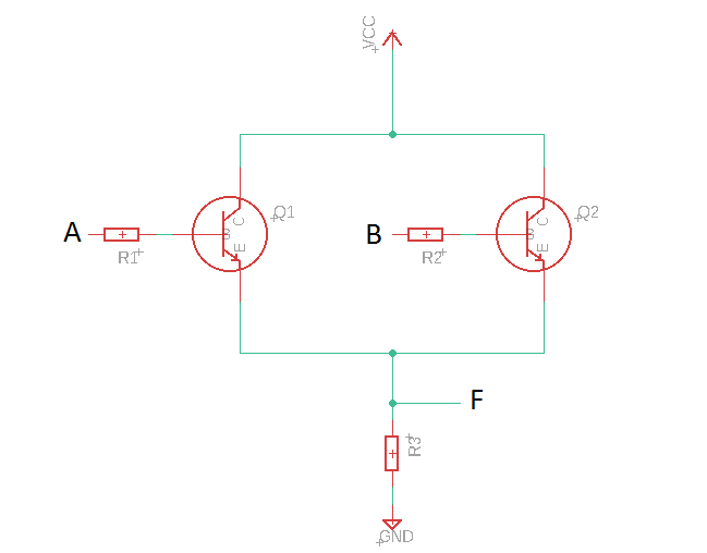
According to the circuit diagram, a high voltage will be present on the output “F” whenever any one of the two transistors is switched on, i.e., whenever A or B is high.
Simple OR Gate Circuit

Here is a simple OR gate circuit with a 2-input OR gate which has an LED connected to its output. The LED will light up even if one of the two inputs is high.
Multiple Gate Design
We can design circuits with multiple OR gates incorporated in them. Consider a car alarm system that goes off when any of the four doors is not properly shut. For the alarm to go off, it needs one of the doors to send a “high” signal. We can connect the four doors through OR gates and connect the output to the alarm, as shown below:
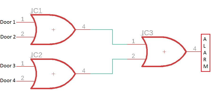
If the doors are closed, they will be at logic level 0, but if they are open, they will set the OR gate’s input at a high voltage, i.e., logic level 1. Even if one of the doors is open, it will set one of the inputs of IC3 to 1 and activate the alarm; this is a simple illustration of how you can incorporate multiple gates in the same circuit for real-life applications.
NOR Gate
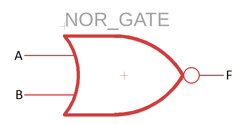
NOR is a short form for (Not-OR), which implies that a NOT gate is added at the OR gate’s output to form the NOR gate (indicated by a bubble after the OR gate symbol). NOT is an inverting gate, which means that it will generate 1 at the output if the input is 0, and vice versa. To make it easier to understand, you can consider the NOR gate to work exactly opposite the OR gate.
NOR will return a logic level 0 when any of its inputs are 1; otherwise, it will remain at logic level 1. The NOR gate performs logical addition and then inverts the results, or it first inverts the inputs and then performs logical multiplication. We can write the equation as:
F = A + B
The overline indicates the “NOT” function. This equation generates the following truth table:
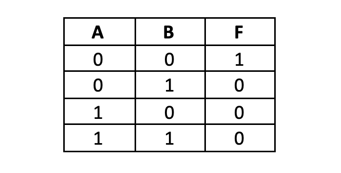
Internal Working
To explain a NOR gate’s internal working, consider two transistors connected in parallel with their emitters connected to the ground and their collectors joint to a resistor, connecting them to the voltage supply Vcc. The two inputs, A and B, are applied at each of the transistors’ bases, and the output, F, is measured where the two collectors meet.
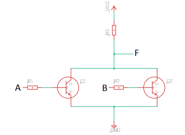
Here, the NOR gate will always generate a low output except when both the transistors are cutoff (at logic level 0).
Simple NOR Gate Circuit
We can use the NOR gate to light up a bulb as we did previously. Here’s how the circuit would look like:

The two inputs can be any conditions that you want to meet to turn the lights ON because typically, the light will remain off (at logic level 0). Only when the NOR gate receives two 0’s at its input will it turn the light on.
Multiple Gate Design
We can incorporate multiple NOR gates in a circuit if we need a 4-input NOR gate. But the catch here is that this time we won’t be using 3 transistors; instead, we will use 5 NOR gates as shown below:
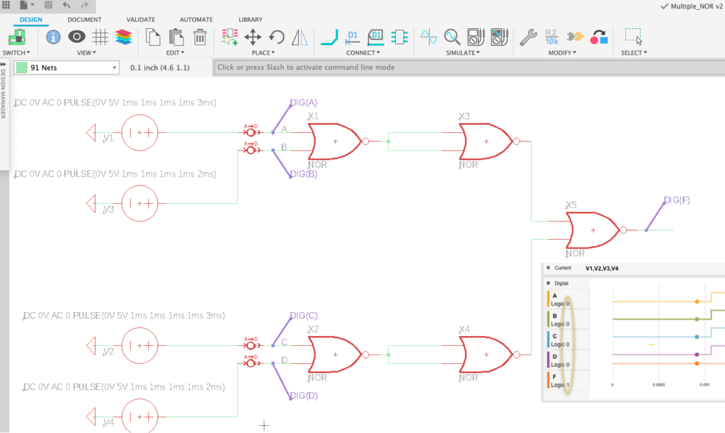
If A and B are 0, then X1 will generate a High output i.e. logic level 1, which is then fed as an input to both the terminals of X3, rendering a 0 as the output, which implies that since A and B are 0, the input to X5 is also the same. The intermediate gates only perform an inverting function so that the final gate gets the same inputs present at A, B, C, and D.
Multiplexers
Multiplexers (or MUX) allow multiple analog or digital signals to travel through a single output. They are commonly used in telecommunications, where multiple calls or text messages need to travel on the same network, i.e. the same output terminal.
A multiplexer has multiple input lines and a single output terminal. It selects the inputs one-by-one and allows them to use the output line for a specific time. A selector line allows you to select which input you want to transmit on the output. Here is what a multiplexer IC looks like:
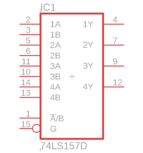
This is an IC with 4 multiplexers, each having two input lines and one output line (2:1 MUX), called a quad 2:1 MUX IC. Each of the input lines is denoted by A and B. For instance, the first multiplexer’s input lines are 1A and 1B, and 1Y represents the output line. The selection line is indicated by A/B, which means that it will select A if it is set at 0 and select B is supplied with a high logic level.
The input lines (M) and the number of selection lines (n) are related through a simple formula:
M = 2n
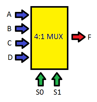
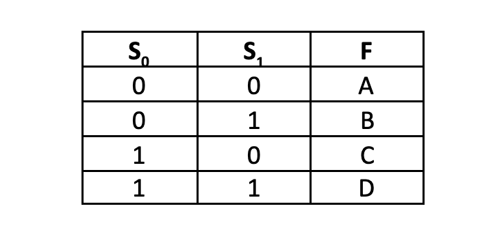
For instance, if we need 4 input lines, then the number of selection lines required are n=2 i.e. for a 4:1 MUX, the number of selection lines required is 2. Each of the four inputs would be selected based on the 0 and 1 combination of the two selection lines. We can name the inputs as A, B, C, D, the selection lines S0 and S1, and see what the truth table for a 4:1 MUX looks like:
Multiplexer Circuit Examples
Multiplexers are used in many applications such as communication systems, telephone networks, computer processing, and satellite communications. According to a specific selection scheme, they allow multiple input signals to travel on the same output line.
Similarly, we have an example of an adjustable-gain amplifier, which uses a multiplexer to adjust an operational amplifier’s gain. Its gain depends on the input and feedback resistor values. One way to adjust the gain is to add a multiplexer on the feedback circuit, where each MUX input would have a different resistance value attached to it. The selection lines would be used to adjust the feedback resistance and change the overall amplifier gain. We can do so by designing a circuit like this:
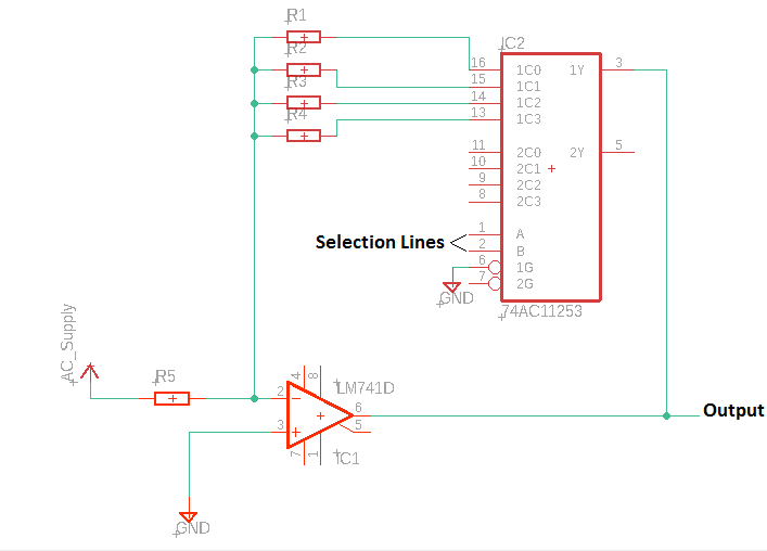
We have used a Dual 4:1 MUX IC together with LM741 op-amp IC. The user can choose from the resistors R1, R2, R3, and R4, by applying a suitable input at the selection lines. You can adjust the gain of the op-amp by using a multiplexer.
Logic gates and multiplexers can be used in many ways to design useful electronic circuits for various applications. Now that you understand how they work, and you’re ready to use them; however you like.
Logic gates and multiplexers are the heart of digital electronic circuits. They work on the simple principle of 1s and 0s, which is very easy to understand and implement for beginners and experienced professionals. They are used in many electronic circuits such as microcontrollers, computer circuitry, microprocessors, digital signal processors, and several other logic circuits. The main concept behind these circuits is Boolean algebra, which is very simple to understand; hence, working with 1s and 0s might sound like a simple job, but the combination of these numbers has led to the creation of many magnificent and wonderful electronic devices and processes.
Ready to incorporate AND, OR and NOR gates into your next circuit design? Fusion 360 gives you access to comprehensive electronics and PCB design tools in one product development platform—try it today!