Explore the main takeaways of our webinar with MacroFab that delved into considerations for designing manufacturable PCBs.
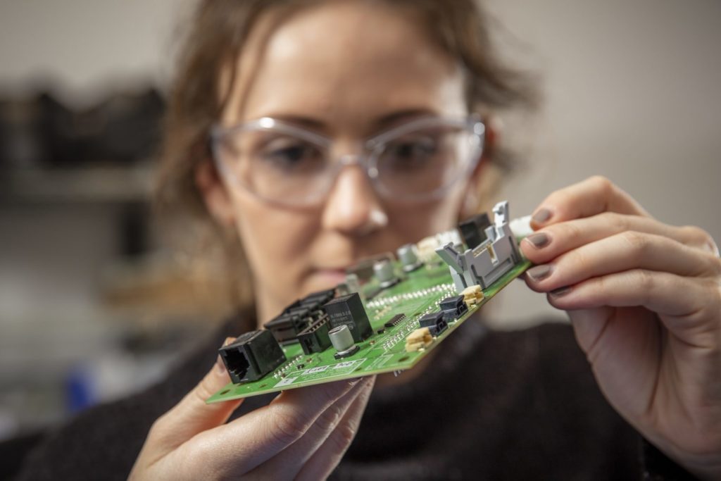
Demand for smart devices and other electronics continues to skyrocket, and with it, the need to design PCBs that can be manufactured successfully, fit within budget, and perform well. In a joint webinar with MacroFab, an innovative contract manufacturer based in Houston, Texas, we explored essential best practices for designing successful PCBs. MacroFab founder and Chief Product Officer Chris Church, who has 20 years of experience in software, electronics, and robotics, led the presentation. In this article, we’ll recap the webinar, giving you key information to consider when designing manufacturable PCBs.
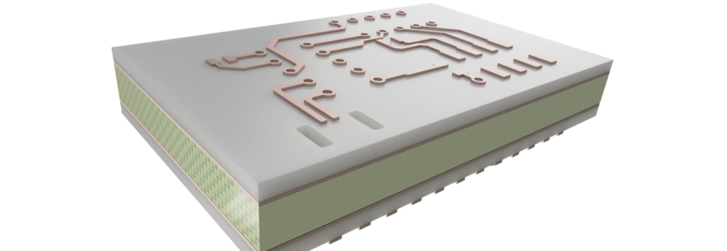
The Anatomy of a PCB
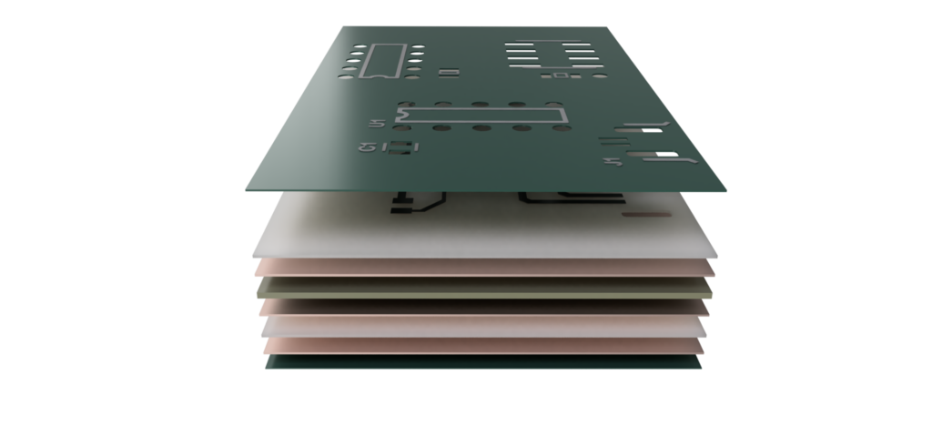
Every PCB has one or more copper layers, which transmit the signal, with isolating substrates in between each layer. The substrates are typically made from flame-resistant fiberglass with a certain temperature threshold depending on the needs of the application or manufacturing method. FR4-175, for example, would withstand 175°C before experiencing delamination or damage.
Substrates may be core, a rigid fiberglass structure with a copper coating on one or both sides, or prepreg, a fiberglass sheet with hardened but uncured resin inside. Prepreg is often used between core or copper layers to prevent air pockets that can damage the PCB when trapped moisture boils and explodes.
PCBs also have drills, including copper-plated conductive vias for transmitting signal and non-plated and nonconductive drills for mounting holes. Then, on top of the copper traces is the solder mask, which protects the copper from oxidization and prevents solder from flowing where it shouldn’t. The mask may be applied with hot air solder leveling (HASL) or electroless nickel immersion gold (ENIG).
Finally, the PCB has a silkscreen, which is far more than decorative. It gives machine operators and board assembly teams a critical visual reference they can match to documentation. Together, all of these features form the “stackup” of the PCB.
Tradeoffs of Board Thickness
You can determine the thickness of a PCB by the specifications of each layer in the stackup, or the collective thickness of the copper, cores, and prepreg. The primary concern about thickness is the eventual application of the device your PCB will control. For example, if it’s a small wearable or a device that experiences a lot of vibration, a thicker board may be necessary.
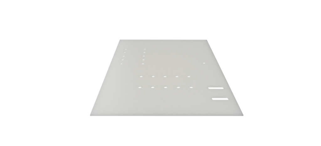
The standard thickness for PCBs is 1.57 mm, or 0.063 inches. Of course, you can go thicker or thinner than this, but there are consequences. For example, at the top end, you might see a PCB that is 12 mm thick, which is exceptionally challenging to manufacture due to the number of layers involved and the overall bulk.
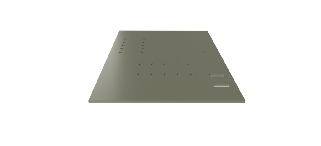
At the other end, you might see a PCB that is less than 1 mm thick for a watch or a similarly small design where space is at a premium. The tradeoff here is cost because these PCBs require custom workholding fixtures to prevent bowing, warping, and other damage during manufacturing, where nearly every step exerts pressure on the board. Custom fixtures might cost several thousand dollars apiece, so costs will add up quickly for a high-throughput board that needs 20 of them. Excessively thin PCBs also tend to flex after assembly, which can cause cracks and breaks in the solder joint that result in defects.
The manufacturer can provide guidance for the thickness of the stackup because they know from experience what thickness aligns with which design goals and how the processes and equipment they use may effect impedance and signal handling. Reaching out to the fabricator during the design process is especially important for high-performance PCBs or custom thicknesses.
The key takeaway here is that you can design anything, but that doesn’t mean it will be manufacturable or fit within your budget. Trust your fabricator to help you understand the tradeoffs and provide guidance before you get to the manufacturing stage.
The Physics of Copper
Copper is, of course, what makes the electrical connections between components in the PCB. Copper is typically described in terms of its weight—one ounce or two-ounce copper. In this case, weight is a measure of thickness, or how thick the copper will be for one square foot of it to weigh one ounce, which is 35 micrometers thick. Two-ounce copper is therefore 70 micrometers thick. Of course, you can use thicker or thinner copper than one or two ounces, but the price difference will be significant.
When you think about the final thickness of copper, remember that virtually every fabricator starts with the thinner foil and then electroplates it with additional copper to reach the target thickness before etching. This makes it easier to control the final thickness and allows the fabricator to keep fewer core variants on hand.
Another important point is that traces in actual practice are not perfectly rectangular. Instead, they are trapezoidal because the top edge near the photo resist spends more time in etch than the bottom layer. In other words, trace width is not uniform.
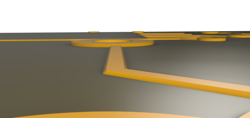
For both of these reasons, a PCB design can’t mix copper thicknesses on the same layer. Fabricators have clear design rules about minimum trace width and spacing, and these rules change depending on copper thickness. The thicker the copper, the wider it needs to be to provide adequate current-carrying capacity. Also, if you run too much current through too thin a trace, you risk melting the copper. Generally, you should move high-speed signal traces to an inner layer, which will have a thinner copper, and move high-current traces to outer layers, where it is easier to use thicker copper.
Ignoring minimum spacing rules is a surefire way to ruin a PCB. If two traces are too close together, you run the risk of them blending and creating acid traps that will break the link. Remember, every manufacturing process has tolerances, and the more you stack those tolerances up by always hitting the minimum allowance, the higher the risk of rejects.
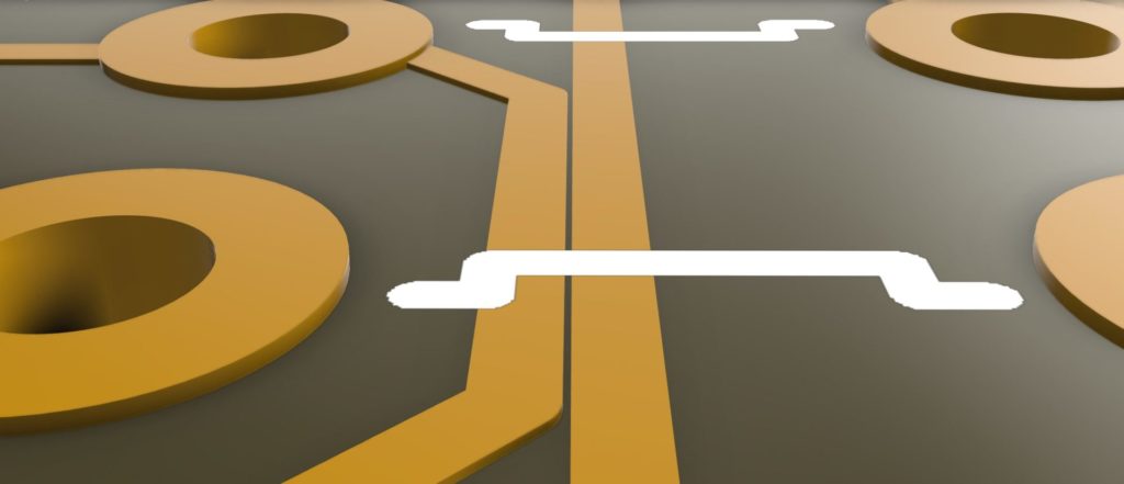
This principle also applies to the spacing between copper and board edge, which is critical. If you stray into the “keep out” area, it can damage the edge traces when the boards are separated.
Incorporating Vias
To create a via, drilling is done after copper etching. Parts of the via include the annular ring (the copper around the via), the drill hole, and the copper plating inside the hole.
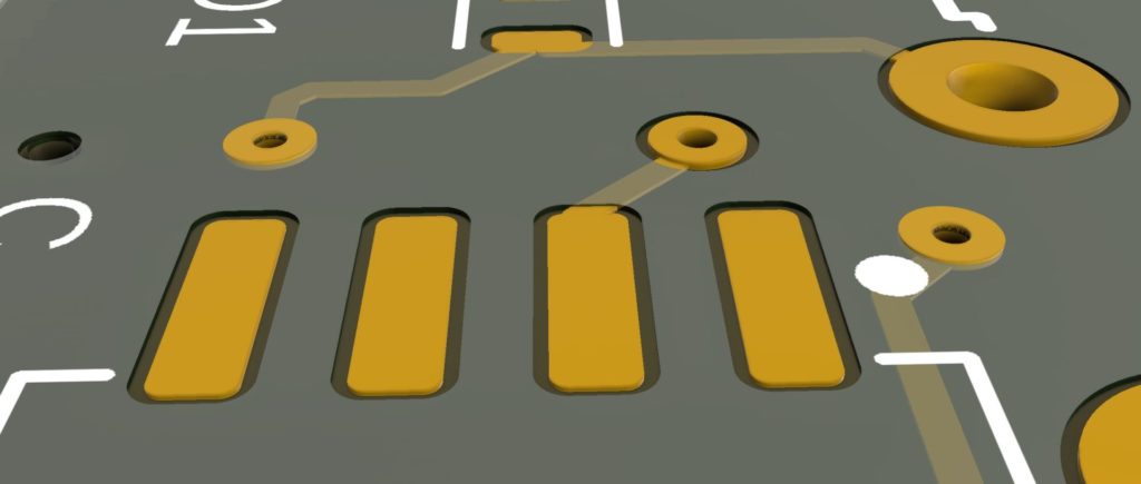
There is also solder mask clearance. Un-tented vias have exposed annular rings. With tented vias, the solder mask covers the ring. Tented vias are preferable because they provide more area for the silkscreen and protect the via from taking in additional solder, which happens occasionally and can change the electrical properties of the via.
Keep in mind that the drill position has tolerance and will not always be perfectly centered. Therefore, it’s vital to adhere to minimum annular ring width rules that allow some travel in the drill bit while maintaining the copper connection.
Copper must surround vias at the entrance and exit points to carry the current. Therefore, non-plated through-holes will not have copper on both sides, although copper may exist on one side to accommodate a screw head support. If you don’t want these plated, it’s important to create a separate drill file for the fabricator to follow.

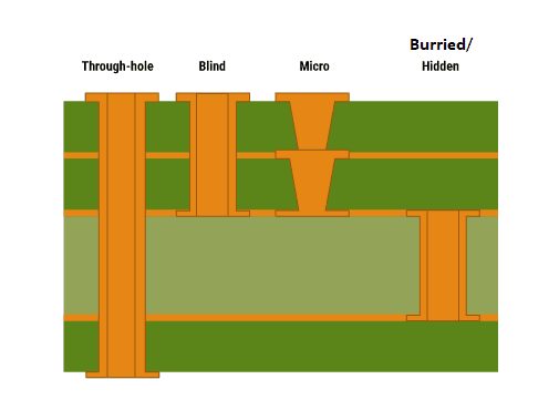
The three most common types of vias are the standard, buried, and blind. A standard via goes through all layers of the board. A buried via goes through two or more inner layers but not outer layers. A blind via starts on an outer layer but does not go all the way through.

Blind and buried vias are much more expensive because they require more drilling operations. However, back drilling is a way to get the advantage of a blind via, which can carry signal through some layers but not to the bottom. Back drilling is when the copper is drilled out of a standard via from one side, rendering enough layers blind so the signal doesn’t pass through.
One final type of via is the micro via, which only goes through a single layer with a 0.25 mm or less hole, so the ratio of depth to width is 1:1. These are used in high-density interconnect (HDI) boards.
It’s also important to consider vias-in-pads (VIPs), which should generally be avoided but are useful to solve two specific problems. One is escape-routing BGAs when minimum spacing rules do not allow vias between pads. The other is for heat-sinking or current-carrying capacity.
You should generally avoid VIPs because they elevate the risk of performance issues if not filled correctly. VIPs must either be filled with non-conductive epoxy for signal or current-carrying purposes and conductive epoxy for heat sinking. Epoxy fills will add between 20% and 40% to your total cost.
Finally, if you use VIPs for escape-routing BGAs, they must be capped to avoid solder affecting BGA performance, which can lead to failures. Again, capping adds a lot of time and cost but is critical to the final quality of the PCB in those instances when you need to use a VIP.
In summary, you can design any PCB, but not every design is manufacturable. Following these best practices will better position you to produce a quality PCB that performs as expected — without blowing up your budget. Watch the full webinar below, and download Fusion 360 for an integrated electronics design experience.
