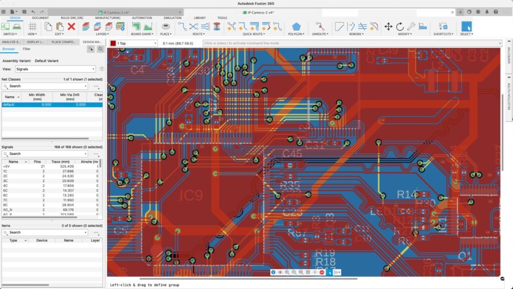
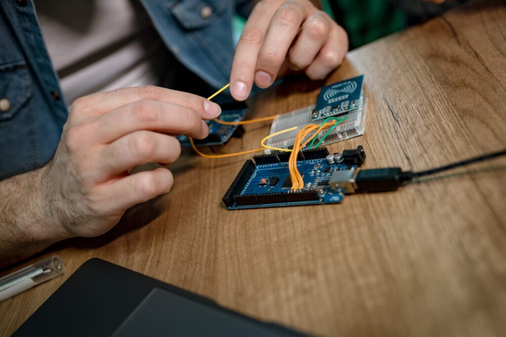
Let’s look at the basics of PCB design for wireless technologies, best practices, and challenges when creating wireless products.

Introduction to PCB Layout Design for Wireless Technologies
In recent years, the demand for wireless communication technologies like Bluetooth and Wi-Fi has grown exponentially. These technologies have become essential to our lives, enabling us to connect and transfer data seamlessly between various devices. As a result, designing and manufacturing cutting-edge wireless products require a strong understanding of printed circuit board (PCB) layout design.
As an experienced design engineer, I have encountered numerous challenges and opportunities while working on PCB layout design for wireless technologies. In this article, I will share my insights and expertise on mastering PCB layout design for Bluetooth and Wi-Fi-enabled products. We will explore the basics of these wireless technologies. As well as the importance of PCB layout design in such products, key considerations, best practices, and everyday challenges.
Understanding the Basics of Bluetooth and Wi-Fi Technologies

Before delving into the specifics, it’s essential to understand the fundamental principles of Bluetooth and Wi-Fi technologies. Bluetooth technology is a short-range wireless communication protocol primarily for transferring data between devices. It operates in the 2.4 GHz industrial, scientific, and medical (ISM) frequency band. It uses frequency-hopping spread spectrum (FHSS) and adaptive frequency hopping (AFH) techniques to maintain robust connections and avoid interference.
Wi-Fi is a wireless networking technology that connects devices to the Internet and local area networks (LANs). Wi-Fi operates in the 2.4 GHz and 5 GHz frequency bands. It uses orthogonal frequency-division multiplexing (OFDM) and multiple-input, multiple-output (MIMO) techniques for high-speed data transmission. Bluetooth and Wi-Fi technologies have unique characteristics, requirements, and challenges to address during the PCB layout design process.
Importance of PCB Layout Design in Bluetooth and Wi-Fi Enabled Products

The quality of a PCB layout can significantly impact the performance, reliability, and overall success of a wireless product. A well-designed PCB layout ensures optimal signal integrity, minimal interference, and efficient power management. All of which are crucial for maintaining stable, high-performing wireless connections.
In Bluetooth and Wi-Fi-enabled products, the PCB layout design plays an even more critical role. This is due to high-frequency signals, sensitive RF components, and complex antenna systems. A poorly designed PCB layout can lead to signal degradation, increased noise levels, and reduced wireless connectivity range. Therefore, following best practices and design guidelines for wireless applications is essential for a successful PCB layout design.
Critical Considerations for Designing PCB Layouts for Wireless Technologies
Designing PCB layouts for wireless applications involves several critical factors that must be considered to ensure optimal performance and reliability. Some of the key considerations include:
- Layer Stackup and Material Selection: The choice of PCB material and layer stack-up can significantly impact signal integrity. As well as power distribution, and thermal management in wireless applications. High-frequency materials like Rogers or FR-4 with low dielectric constant and low loss tangent are recommended for minimizing signal loss and maintaining impedance control.
- RF Component Placement: The placement of RF components, such as antennas, filters, and amplifiers, is crucial in minimizing signal interference and achieving optimal signal integrity. Careful attention must be paid to the proximity of RF components to other signal and power components and the routing of RF traces and ground planes.
- Power Distribution and Grounding: Efficient power distribution and grounding are essential for maintaining stable wireless connections and minimizing noise in Bluetooth, and Wi-Fi-enabled products. A proper power distribution network (PDN) and ground planes are crucial to ensure stable voltage levels and reduce electromagnetic interference (EMI).
PCB Layout Design Best Practices for Bluetooth Circuit Boards
When designing a Bluetooth circuit board, following certain best practices to ensure optimal performance and reliability is essential. Some of these best practices include:
- Maintain Impedance Control: Bluetooth signals are susceptible to impedance mismatches, which can lead to signal reflection and degradation. Maintaining controlled impedance throughout the PCB layout is vital by using proper trace widths, spacing, and dielectric materials.
- Minimize RF Trace Lengths: To maintain signal integrity and minimize signal loss, it’s essential to keep RF trace lengths as short as possible. This helps reduce the impact of parasitic capacitance and inductance and minimize the chances of cross-talk and interference.
- Proper Shielding and Isolation: Shielding and isolation are critical for minimizing EMI and ensuring reliable wireless connections in Bluetooth circuit boards. It’s essential to use appropriate shielding techniques. These include ground planes, shielding cans, and ferrite beads, to minimize interference from other components and external sources.
Wi-Fi Circuit Design: Types, Chips, and On-Board Considerations
Wi-Fi circuit design involves various types of Wi-Fi chips and onboard considerations for a successful PCB layout. Some common Wi-Fi types include single-band, dual-band, and tri-band Wi-Fi. These operate at different frequency bands and offer varying levels of performance and range.
When selecting Wi-Fi chips for your design, it’s essential to consider factors such as power consumption, data rate, and integration with other components on the board. Some popular Wi-Fi chipsets include Broadcom, Qualcomm, and Texas Instruments. All of which offer a wide range of features and capabilities to suit different application requirements.
For onboard Wi-Fi considerations, it’s crucial to follow best practices for RF component placement, trace routing, and antenna design to ensure optimal performance and signal integrity. Additionally, proper power management and thermal considerations must be addressed to maintain stable Wi-Fi connections and prolong the product’s life.
Antenna Selection and Placement for Wi-Fi and Bluetooth PCBs
Antenna selection and placement are critical in determining the range, signal strength, and overall performance of Wi-Fi and Bluetooth-enabled products. Various types of antennas are available for wireless applications, such as chip antennas, PCB trace antennas, and external antennas. The choice of the antenna depends on factors such as desired range, form factor, and cost.
Proper antenna placement is crucial for minimizing interference and maximizing signal strength. Keeping the antenna away from other components, metallic objects, and high-speed digital signals is essential. This helps prevent signal degradation and reduced range. Proper impedance matching and ground plane design must also be considered for optimal antenna performance.
Testing and Validation of Wireless PCB Layout Designs

Once the PCB layout design for a wireless application is complete, testing and validating the design is essential to ensure optimal performance and reliability. Some of the standard tests and validation techniques include:
- Signal Integrity Analysis: This involves simulating the PCB layout and analyzing the signal behavior to identify potential issues. These could include impedance mismatches, signal loss, and cross-talk. Tools like SPICE and HyperLynx can be used for signal integrity analysis.
- EMI and EMC Testing: Electromagnetic interference (EMI) and electromagnetic compatibility (EMC) testing are critical for ensuring the wireless product meets regulatory requirements and operates reliably in its intended environment. These tests involve measuring the radiated emissions, conducted emissions, and susceptibility to external interference.
- Antenna Performance Testing: This involves measuring the antenna’s radiation pattern, gain, efficiency, and impedance matching to ensure optimal performance and range in the final product.
Common Challenges and Solutions in Bluetooth and Wi-Fi PCB Layout Design
Designing PCB layouts for Bluetooth and Wi-Fi-enabled products can be challenging. This is due to the complex nature of wireless technologies and the need for precise RF component placement, routing, and grounding. Some of the common challenges and their solutions include:
- Signal Interference: Minimizing signal interference is crucial for maintaining stable wireless connections and ensuring optimal performance. This can be achieved by carefully placing RF components, using proper shielding techniques, and optimizing trace routing and grounding.
- Thermal Management: Managing heat dissipation is essential for prolonging the life of wireless products and maintaining stable Wi-Fi and Bluetooth connections. This can be achieved by using proper thermal vias and heat sinks and selecting components with low power consumption.
- Design Complexity: The complexity of wireless technologies and the need for precise RF component placement can make PCB layout design challenging. Using advanced design tools, following best practices, and leveraging the expertise of experienced design engineers can help overcome these challenges and achieve a successful PCB layout.
Future Trends Wireless PCB Layout Design for Wireless Technologies
In conclusion, mastering PCB layout design for cutting-edge Bluetooth and Wi-Fi-enabled products is essential for ensuring optimal performance, reliability, and success in today’s competitive wireless market. By the basics of wireless technologies, following best practices, and addressing key design considerations, engineers can create high-quality PCB layouts that meet the requirements of modern wireless applications.
The demand for more sophisticated and integrated PCB layouts will only increase as wireless technologies evolve. Future trends in wireless PCB layout design will focus on further miniaturization, integrating multiple wireless technologies, and adopting advanced materials and manufacturing techniques. By staying up-to-date with these trends and continuously refining their skills, design engineers can continue creating successful, cutting-edge wireless products.
Ready to get started with PCB design for your next wireless product? Download a free 30-day trial of Autodesk Fusion 360.