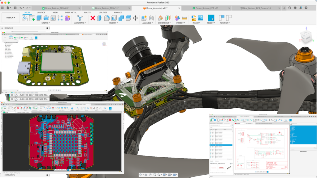
Autodesk Fusion Electronics has evolved into a powerful, intuitive, and high-performance PCB design solution that seamlessly integrates electronics, mechanical CAD, and simulation in one platform. With faster performance, AI-driven automation, and real-time collaboration, Fusion simplifies complex designs, ensuring precision and efficiency from concept to production.
PCB design in Autodesk Fusion
If you’re exploring options for PCB design, Autodesk Fusion electronics should be at the top of your list. This isn’t just another design tool; it’s a game-changer for electronic designers, and if you’re designing consumer products, this is the solution you’ll want to use. Here’s why.
1. Intuitive, high-performance PCB design
Fusion electronics has reached a whole new level, and it’s faster and smarter than ever. Our developers have worked closely with our XD experts to refine the interface, making it far more intuitive and easier to use. But it’s not just about looks. Take a look at these significant performance enhancements:
Instantaneous updates – Thanks to advanced polygon calculations, PCB modifications are applied in real time
Enhanced via stitching – This feature improves signal integrity, thermal management, EMI shielding, and structural strength in PCBs.
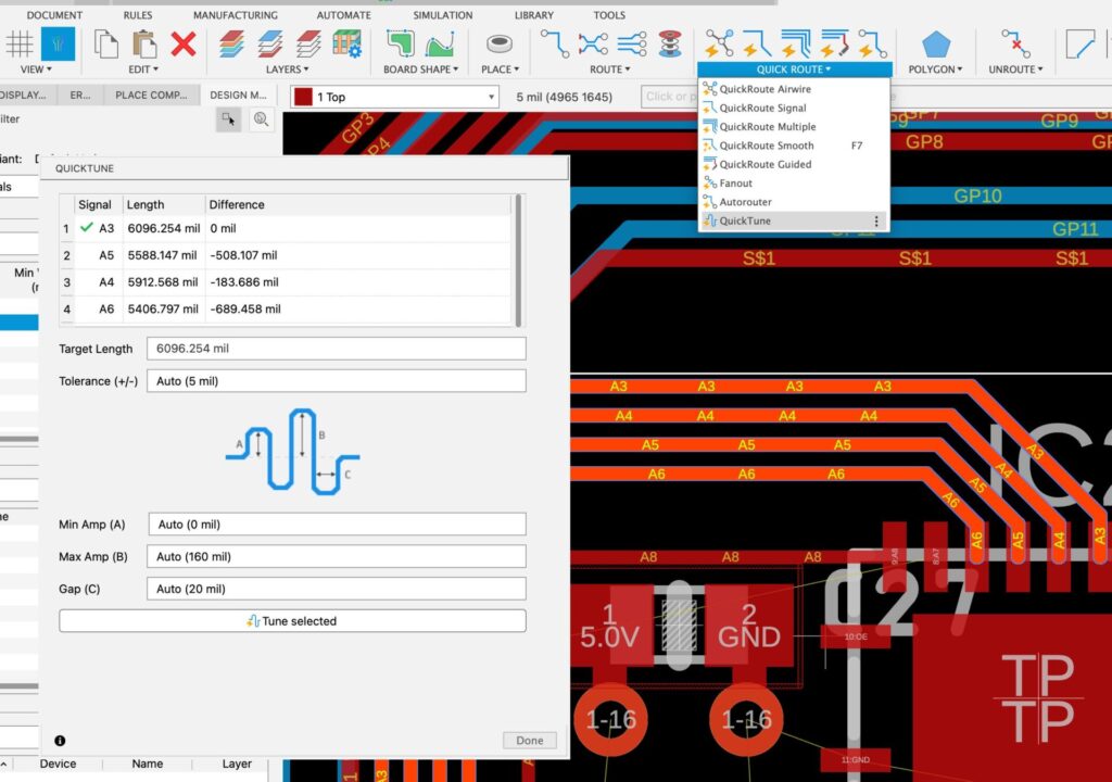
Smarter interactive routing – New automation tools like QuickTune that streamlines length tuning, giving you greater control over trace adjustments.
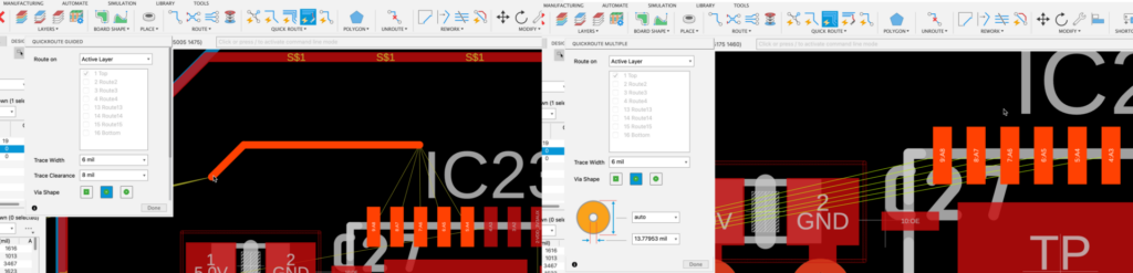
2. QuickRoute: Best-kept secret
There was a recent forum post called QuickRoute the best-kept secret in Autodesk Fusion for electronics —and for good reason. This powerful feature speeds up PCB layout routing by automatically generating or optimizing trace paths with precision and ease. Whether you’re working with a single trace or an entire group of signals, QuickRoute helps streamline your workflow.
Group routing: control and automation
QuickRoute offers two group routing methods:
Automated group routing – Generates the best possible trace path for a selected group of signals.
Guided group routing – Allows you to influence the path while still benefiting from automation.
Guided routing is especially useful for bus routing, where you need to route multiple signals simultaneously while maintaining control over their paths. Personally, I prefer Group Route Guided, as it gives me more flexibility in defining the intended trace paths.
QuickRoute smooth: Clean, efficient traces
One of my favorite tools—one I use daily—is QuickRoute smooth. While I sometimes rely on the Autorouter and refine the results afterward, QR smooth takes routed traces and optimizes them by finding a shorter path with fewer bends.
For large designs, this tool is invaluable. Routing is an art, and while there’s no single “right” way to do it, QuickRoute Smooth helps achieve cleaner, more efficient layouts.
QR fanout: Simplifying ground plane connections
QR Fanout is an essential tool used to create fanouts of specific signals over short distances, ending in a via. A common use case is connecting a ground signal to a ground plane, ensuring solid electrical performance with minimal manual effort.
QR airwire vs. QR signal: Routing made simple
QR airwire – Automatically routes a single airwire, which is especially useful for short-distance connections, such as bypass capacitors placed near components.
QR signal – Routes all traces associated with a specific signal name, making it a powerful option for managing complex connections across the board.
By leveraging QuickRoute, you can speed up PCB layout while maintaining full control over trace paths. Whether you’re routing manually or optimizing an existing design, these tools make the process faster, smoother, and more precise.
QuickTune
I want to end this section with our latest member of the QR family which is QuickTune. QuickTune is our automated length-matching tool. It can be used for a trace of a group of selected traces. If you choose a group of traces, it will attempt to meander all the selected traces to match the longest trace. You can specify the length of the single or group of traces. You can also select the meander’s Min and Max amplitude and gap. A meander is a powerful tool used to facilitate signals to reach their destination, simultaneously guaranteeing the function of the components.
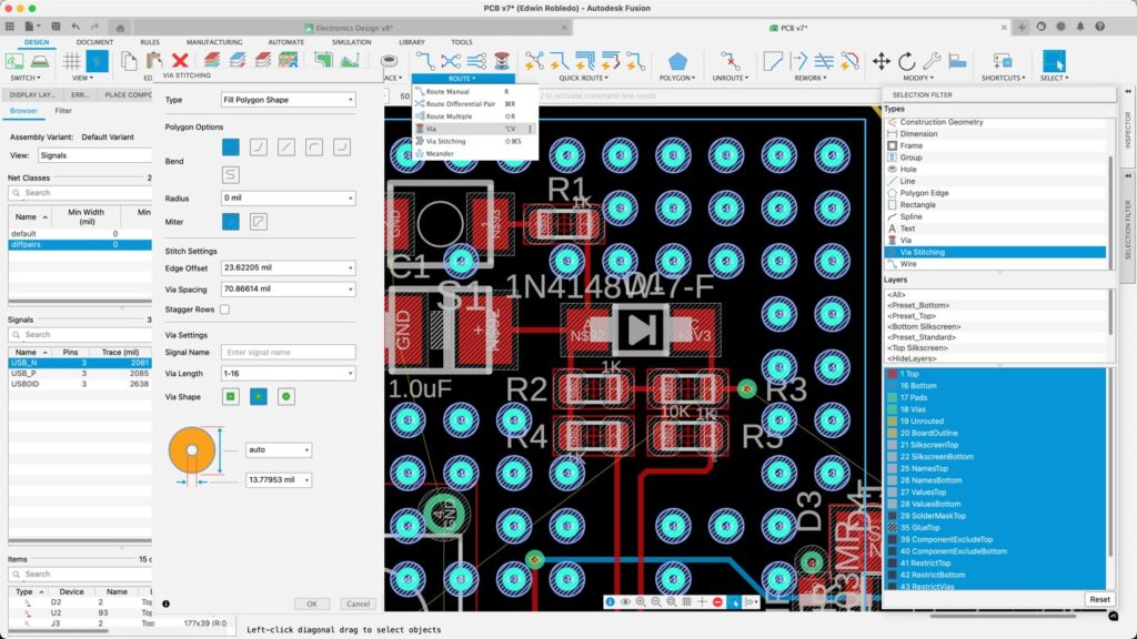
3. Via stitching
Another powerful tool in Fusion Electronics isvia stitching, which enhances PCB design reliability by improving signal integrity, managing heat dissipation, and reducing electromagnetic interference (EMI).
Proper grounding is crucial when designing high-frequency PCBs, and via stitching features in Fusion electronics workspace make this process seamless. One of its key advantages is its intuitive handling. Notably, via stitch is integrated into the selection filter, making it easy to select, resize, or delete as needed.
The via stitching dialog box provides full control over via properties, allowing you to fine-tune parameters such as drill size and placement. Additionally, the design rule check (DRC) mask settings automatically calculate the necessary mask adjustments, ensuring compliance with your design constraints.
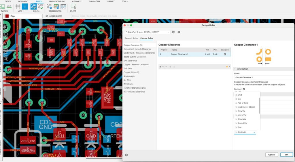
4. Advanced design rule capabilities
Fusion electronics redefines PCB design rules with a flexible, structured system that distinguishes design preferences—global PCB settings like layer stack-ups—from design rules, which enforce specific manufacturing constraints. This approach enables engineers to establish precise guidelines early in the design process, minimizing rework and enhancing workflow efficiency.
General rules define fundamental constraints such as trace widths and clearances, ensuring manufacturability while allowing for controlled overrides when necessary. Net classes provide targeted exceptions for specific circuit segments, such as wider traces for power rails, enhancing both performance and design integrity.
For even greater control, custom rules allow designers to apply constraints to specific layers, components, or nets—essential for managing the complexities of advanced PCB designs. Meanwhile, Live design rule checking (DRC) delivers real-time feedback, proactively detecting errors and ensuring compliance with industry standards. This intelligent rule-checking system streamlines the PCB design process, improving both accuracy and efficiency.
5. All-in-one integration, means easier collaboration
When mechanical and electronics engineers don’t work in sync, it can lead to costly mistakes—like discovering too late that a circuit board doesn’t fit the enclosure. Fixing these issues after the fact can mean wasted time, blown budgets, and frustrating delays. A connected workflow lets teams quickly adapt board outlines, check for interferences, and make real-time changes before it’s too late. Without a realistic 3D model, you’re designing in the dark, risking expensive rework and missed deadlines. When teams collaborate seamlessly, they save time, money, and headaches—getting great products to market faster. This is where Fusion truly shines.
Fusion electronics brings electronics and mechanical design together in one solution.
Built-in 3D modeling – Easily visualize and adjust PCB designs within mechanical enclosures.
Powerful collaboration tools – Teams can work together in real-time without software silos.
Collaborative-based workflows – Access and manage design data from anywhere.
Eliminates file transfers – No need for back-and-forth exchanges between ECAD and MCAD tools.
Reduces compatibility issues – Ensures smooth data flow between electronic and mechanical designs.
Prevents fit & clearance errors – Verify that PCB components align correctly within enclosures.
Construction lines in the mechanical design workspace will exist in the PCB editor, which guides the PCB design workspace.
Electronic component placement can be fine-tuned in the Mechanical Design workspace, which will synchronize with the PCB editor.
Changes to the design are adopted in moments by all involved workspaces.
Electronics design made easy with Autodesk Fusion
Fusion electronics is more than just software; it’s a solution for designers like you who demand performance, precision, and ease of use. It’s the smarter choice for consumer product seamlessly integrating PCB design, mechanical CAD, and simulation in a single platform. Furthermore, Fusion’s collaboration tools provide a centralized platform for managing design iterations and feedback from multiple stakeholders.
Whether you need cutting-edge features like QuickTune, via stitching or complex design rules due to design complexity and fabrication restrictions, Fusion Electronics equips you with everything you need to bring your ideas to life.
If you’re serious about taking your PCB design to the next level, try Autodesk Fusion Electronics. Trust me, you’ll wonder how you ever managed without it.
Full-access Fusion Trial
Unlock all of Fusion's advanced features and functionality - free for 30 days.
By clicking subscribe, I agree to receive the Fusion newsletter and acknowledge the Autodesk Privacy Statement.
Success!
______
Cookie preferences
Your privacy is important to us and so is an optimal experience. To help us customize information and build applications, we collect data about your use of this site.
Learn more about the Third-Party Services we use in each category, and how we use the data we collect from you online.
Strictly necessary – required for our site to work and to provide services to you
Qualtrics
We use Qualtrics to let you give us feedback via surveys or online forms. You may be randomly selected to participate in a survey, or you can actively decide to give us feedback. We collect data to better understand what actions you took before filling out a survey. This helps us troubleshoot issues you may have experienced. Qualtrics Privacy Policy
Akamai mPulse
We use Akamai mPulse to collect data about your behavior on our sites. This may include pages you’ve visited, trials you’ve initiated, videos you’ve played, purchases you’ve made, your IP address or device ID, and your Autodesk ID. We use this data to measure our site performance and evaluate the ease of your online experience, so we can enhance our features. We also use advanced analytics methods to optimize your experience with email, customer support, and sales. Akamai mPulse Privacy Policy
Digital River
We use Digital River to collect data about your behavior on our sites. This may include pages you’ve visited, trials you’ve initiated, videos you’ve played, purchases you’ve made, your IP address or device ID, and your Autodesk ID. We use this data to measure our site performance and evaluate the ease of your online experience, so we can enhance our features. We also use advanced analytics methods to optimize your experience with email, customer support, and sales. Digital River Privacy Policy
Dynatrace
We use Dynatrace to collect data about your behavior on our sites. This may include pages you’ve visited, trials you’ve initiated, videos you’ve played, purchases you’ve made, your IP address or device ID, and your Autodesk ID. We use this data to measure our site performance and evaluate the ease of your online experience, so we can enhance our features. We also use advanced analytics methods to optimize your experience with email, customer support, and sales. Dynatrace Privacy Policy
Khoros
We use Khoros to collect data about your behavior on our sites. This may include pages you’ve visited, trials you’ve initiated, videos you’ve played, purchases you’ve made, your IP address or device ID, and your Autodesk ID. We use this data to measure our site performance and evaluate the ease of your online experience, so we can enhance our features. We also use advanced analytics methods to optimize your experience with email, customer support, and sales. Khoros Privacy Policy
Launch Darkly
We use Launch Darkly to collect data about your behavior on our sites. This may include pages you’ve visited, trials you’ve initiated, videos you’ve played, purchases you’ve made, your IP address or device ID, and your Autodesk ID. We use this data to measure our site performance and evaluate the ease of your online experience, so we can enhance our features. We also use advanced analytics methods to optimize your experience with email, customer support, and sales. Launch Darkly Privacy Policy
New Relic
We use New Relic to collect data about your behavior on our sites. This may include pages you’ve visited, trials you’ve initiated, videos you’ve played, purchases you’ve made, your IP address or device ID, and your Autodesk ID. We use this data to measure our site performance and evaluate the ease of your online experience, so we can enhance our features. We also use advanced analytics methods to optimize your experience with email, customer support, and sales. New Relic Privacy Policy
Salesforce Live Agent
We use Salesforce Live Agent to collect data about your behavior on our sites. This may include pages you’ve visited, trials you’ve initiated, videos you’ve played, purchases you’ve made, your IP address or device ID, and your Autodesk ID. We use this data to measure our site performance and evaluate the ease of your online experience, so we can enhance our features. We also use advanced analytics methods to optimize your experience with email, customer support, and sales. Salesforce Live Agent Privacy Policy
Wistia
We use Wistia to collect data about your behavior on our sites. This may include pages you’ve visited, trials you’ve initiated, videos you’ve played, purchases you’ve made, your IP address or device ID, and your Autodesk ID. We use this data to measure our site performance and evaluate the ease of your online experience, so we can enhance our features. We also use advanced analytics methods to optimize your experience with email, customer support, and sales. Wistia Privacy Policy
Tealium
We use Tealium to collect data about your behavior on our sites. This may include pages you’ve visited, trials you’ve initiated, videos you’ve played, purchases you’ve made, and your IP address or device ID. We use this data to measure our site performance and evaluate the ease of your online experience, so we can enhance our features. We also use advanced analytics methods to optimize your experience with email, customer support, and sales. Tealium Privacy Policy
Upsellit
We use Upsellit to collect data about your behavior on our sites. This may include pages you’ve visited, trials you’ve initiated, videos you’ve played, purchases you’ve made, and your IP address or device ID. We use this data to measure our site performance and evaluate the ease of your online experience, so we can enhance our features. We also use advanced analytics methods to optimize your experience with email, customer support, and sales. Upsellit Privacy Policy
CJ Affiliates
We use CJ Affiliates to collect data about your behavior on our sites. This may include pages you’ve visited, trials you’ve initiated, videos you’ve played, purchases you’ve made, and your IP address or device ID. We use this data to measure our site performance and evaluate the ease of your online experience, so we can enhance our features. We also use advanced analytics methods to optimize your experience with email, customer support, and sales. CJ Affiliates Privacy Policy
Commission Factory
We use Commission Factory to collect data about your behavior on our sites. This may include pages you’ve visited, trials you’ve initiated, videos you’ve played, purchases you’ve made, and your IP address or device ID. We use this data to measure our site performance and evaluate the ease of your online experience, so we can enhance our features. We also use advanced analytics methods to optimize your experience with email, customer support, and sales. Commission Factory Privacy Policy
Google Analytics (Strictly Necessary)
We use Google Analytics (Strictly Necessary) to collect data about your behavior on our sites. This may include pages you’ve visited, trials you’ve initiated, videos you’ve played, purchases you’ve made, your IP address or device ID, and your Autodesk ID. We use this data to measure our site performance and evaluate the ease of your online experience, so we can enhance our features. We also use advanced analytics methods to optimize your experience with email, customer support, and sales. Google Analytics (Strictly Necessary) Privacy Policy
Typepad Stats
We use Typepad Stats to collect data about your behaviour on our sites. This may include pages you’ve visited. We use this data to measure our site performance and evaluate the ease of your online experience, so we can enhance our platform to provide the most relevant content. This allows us to enhance your overall user experience. Typepad Stats Privacy Policy
Geo Targetly
We use Geo Targetly to direct website visitors to the most appropriate web page and/or serve tailored content based on their location. Geo Targetly uses the IP address of a website visitor to determine the approximate location of the visitor’s device. This helps ensure that the visitor views content in their (most likely) local language.Geo Targetly Privacy Policy
SpeedCurve
We use SpeedCurve to monitor and measure the performance of your website experience by measuring web page load times as well as the responsiveness of subsequent elements such as images, scripts, and text.SpeedCurve Privacy Policy
Qualified
Qualified is the Autodesk Live Chat agent platform. This platform provides services to allow our customers to communicate in real-time with Autodesk support. We may collect unique ID for specific browser sessions during a chat. Qualified Privacy Policy
Improve your experience – allows us to show you what is relevant to you
Google Optimize
We use Google Optimize to test new features on our sites and customize your experience of these features. To do this, we collect behavioral data while you’re on our sites. This data may include pages you’ve visited, trials you’ve initiated, videos you’ve played, purchases you’ve made, your IP address or device ID, your Autodesk ID, and others. You may experience a different version of our sites based on feature testing, or view personalized content based on your visitor attributes. Google Optimize Privacy Policy
ClickTale
We use ClickTale to better understand where you may encounter difficulties with our sites. We use session recording to help us see how you interact with our sites, including any elements on our pages. Your Personally Identifiable Information is masked and is not collected. ClickTale Privacy Policy
OneSignal
We use OneSignal to deploy digital advertising on sites supported by OneSignal. Ads are based on both OneSignal data and behavioral data that we collect while you’re on our sites. The data we collect may include pages you’ve visited, trials you’ve initiated, videos you’ve played, purchases you’ve made, and your IP address or device ID. This information may be combined with data that OneSignal has collected from you. We use the data that we provide to OneSignal to better customize your digital advertising experience and present you with more relevant ads. OneSignal Privacy Policy
Optimizely
We use Optimizely to test new features on our sites and customize your experience of these features. To do this, we collect behavioral data while you’re on our sites. This data may include pages you’ve visited, trials you’ve initiated, videos you’ve played, purchases you’ve made, your IP address or device ID, your Autodesk ID, and others. You may experience a different version of our sites based on feature testing, or view personalized content based on your visitor attributes. Optimizely Privacy Policy
Amplitude
We use Amplitude to test new features on our sites and customize your experience of these features. To do this, we collect behavioral data while you’re on our sites. This data may include pages you’ve visited, trials you’ve initiated, videos you’ve played, purchases you’ve made, your IP address or device ID, your Autodesk ID, and others. You may experience a different version of our sites based on feature testing, or view personalized content based on your visitor attributes. Amplitude Privacy Policy
Snowplow
We use Snowplow to collect data about your behavior on our sites. This may include pages you’ve visited, trials you’ve initiated, videos you’ve played, purchases you’ve made, your IP address or device ID, and your Autodesk ID. We use this data to measure our site performance and evaluate the ease of your online experience, so we can enhance our features. We also use advanced analytics methods to optimize your experience with email, customer support, and sales. Snowplow Privacy Policy
UserVoice
We use UserVoice to collect data about your behaviour on our sites. This may include pages you’ve visited. We use this data to measure our site performance and evaluate the ease of your online experience, so we can enhance our platform to provide the most relevant content. This allows us to enhance your overall user experience. UserVoice Privacy Policy
Clearbit
Clearbit allows real-time data enrichment to provide a personalized and relevant experience to our customers. The data we collect may include pages you’ve visited, trials you’ve initiated, videos you’ve played, purchases you’ve made, and your IP address or device ID.Clearbit Privacy Policy
YouTube
YouTube is a video sharing platform which allows users to view and share embedded videos on our websites. YouTube provides viewership metrics on video performance. YouTube Privacy Policy
Customize your advertising – permits us to offer targeted advertising to you
Adobe Analytics
We use Adobe Analytics to collect data about your behavior on our sites. This may include pages you’ve visited, trials you’ve initiated, videos you’ve played, purchases you’ve made, your IP address or device ID, and your Autodesk ID. We use this data to measure our site performance and evaluate the ease of your online experience, so we can enhance our features. We also use advanced analytics methods to optimize your experience with email, customer support, and sales. Adobe Analytics Privacy Policy
Google Analytics (Web Analytics)
We use Google Analytics (Web Analytics) to collect data about your behavior on our sites. This may include pages you’ve visited, trials you’ve initiated, videos you’ve played, purchases you’ve made, and your IP address or device ID. We use this data to measure our site performance and evaluate the ease of your online experience, so we can enhance our features. We also use advanced analytics methods to optimize your experience with email, customer support, and sales. Google Analytics (Web Analytics) Privacy Policy
AdWords
We use AdWords to deploy digital advertising on sites supported by AdWords. Ads are based on both AdWords data and behavioral data that we collect while you’re on our sites. The data we collect may include pages you’ve visited, trials you’ve initiated, videos you’ve played, purchases you’ve made, and your IP address or device ID. This information may be combined with data that AdWords has collected from you. We use the data that we provide to AdWords to better customize your digital advertising experience and present you with more relevant ads. AdWords Privacy Policy
Marketo
We use Marketo to send you more timely and relevant email content. To do this, we collect data about your online behavior and your interaction with the emails we send. Data collected may include pages you’ve visited, trials you’ve initiated, videos you’ve played, purchases you’ve made, your IP address or device ID, email open rates, links clicked, and others. We may combine this data with data collected from other sources to offer you improved sales or customer service experiences, as well as more relevant content based on advanced analytics processing. Marketo Privacy Policy
Doubleclick
We use Doubleclick to deploy digital advertising on sites supported by Doubleclick. Ads are based on both Doubleclick data and behavioral data that we collect while you’re on our sites. The data we collect may include pages you’ve visited, trials you’ve initiated, videos you’ve played, purchases you’ve made, and your IP address or device ID. This information may be combined with data that Doubleclick has collected from you. We use the data that we provide to Doubleclick to better customize your digital advertising experience and present you with more relevant ads. Doubleclick Privacy Policy
HubSpot
We use HubSpot to send you more timely and relevant email content. To do this, we collect data about your online behavior and your interaction with the emails we send. Data collected may include pages you’ve visited, trials you’ve initiated, videos you’ve played, purchases you’ve made, your IP address or device ID, email open rates, links clicked, and others. HubSpot Privacy Policy
Twitter
We use Twitter to deploy digital advertising on sites supported by Twitter. Ads are based on both Twitter data and behavioral data that we collect while you’re on our sites. The data we collect may include pages you’ve visited, trials you’ve initiated, videos you’ve played, purchases you’ve made, and your IP address or device ID. This information may be combined with data that Twitter has collected from you. We use the data that we provide to Twitter to better customize your digital advertising experience and present you with more relevant ads. Twitter Privacy Policy
Facebook
We use Facebook to deploy digital advertising on sites supported by Facebook. Ads are based on both Facebook data and behavioral data that we collect while you’re on our sites. The data we collect may include pages you’ve visited, trials you’ve initiated, videos you’ve played, purchases you’ve made, and your IP address or device ID. This information may be combined with data that Facebook has collected from you. We use the data that we provide to Facebook to better customize your digital advertising experience and present you with more relevant ads. Facebook Privacy Policy
LinkedIn
We use LinkedIn to deploy digital advertising on sites supported by LinkedIn. Ads are based on both LinkedIn data and behavioral data that we collect while you’re on our sites. The data we collect may include pages you’ve visited, trials you’ve initiated, videos you’ve played, purchases you’ve made, and your IP address or device ID. This information may be combined with data that LinkedIn has collected from you. We use the data that we provide to LinkedIn to better customize your digital advertising experience and present you with more relevant ads. LinkedIn Privacy Policy
Yahoo! Japan
We use Yahoo! Japan to deploy digital advertising on sites supported by Yahoo! Japan. Ads are based on both Yahoo! Japan data and behavioral data that we collect while you’re on our sites. The data we collect may include pages you’ve visited, trials you’ve initiated, videos you’ve played, purchases you’ve made, and your IP address or device ID. This information may be combined with data that Yahoo! Japan has collected from you. We use the data that we provide to Yahoo! Japan to better customize your digital advertising experience and present you with more relevant ads. Yahoo! Japan Privacy Policy
Naver
We use Naver to deploy digital advertising on sites supported by Naver. Ads are based on both Naver data and behavioral data that we collect while you’re on our sites. The data we collect may include pages you’ve visited, trials you’ve initiated, videos you’ve played, purchases you’ve made, and your IP address or device ID. This information may be combined with data that Naver has collected from you. We use the data that we provide to Naver to better customize your digital advertising experience and present you with more relevant ads. Naver Privacy Policy
Quantcast
We use Quantcast to deploy digital advertising on sites supported by Quantcast. Ads are based on both Quantcast data and behavioral data that we collect while you’re on our sites. The data we collect may include pages you’ve visited, trials you’ve initiated, videos you’ve played, purchases you’ve made, and your IP address or device ID. This information may be combined with data that Quantcast has collected from you. We use the data that we provide to Quantcast to better customize your digital advertising experience and present you with more relevant ads. Quantcast Privacy Policy
Call Tracking
We use Call Tracking to provide customized phone numbers for our campaigns. This gives you faster access to our agents and helps us more accurately evaluate our performance. We may collect data about your behavior on our sites based on the phone number provided. Call Tracking Privacy Policy
Wunderkind
We use Wunderkind to deploy digital advertising on sites supported by Wunderkind. Ads are based on both Wunderkind data and behavioral data that we collect while you’re on our sites. The data we collect may include pages you’ve visited, trials you’ve initiated, videos you’ve played, purchases you’ve made, and your IP address or device ID. This information may be combined with data that Wunderkind has collected from you. We use the data that we provide to Wunderkind to better customize your digital advertising experience and present you with more relevant ads. Wunderkind Privacy Policy
ADC Media
We use ADC Media to deploy digital advertising on sites supported by ADC Media. Ads are based on both ADC Media data and behavioral data that we collect while you’re on our sites. The data we collect may include pages you’ve visited, trials you’ve initiated, videos you’ve played, purchases you’ve made, and your IP address or device ID. This information may be combined with data that ADC Media has collected from you. We use the data that we provide to ADC Media to better customize your digital advertising experience and present you with more relevant ads. ADC Media Privacy Policy
AgrantSEM
We use AgrantSEM to deploy digital advertising on sites supported by AgrantSEM. Ads are based on both AgrantSEM data and behavioral data that we collect while you’re on our sites. The data we collect may include pages you’ve visited, trials you’ve initiated, videos you’ve played, purchases you’ve made, and your IP address or device ID. This information may be combined with data that AgrantSEM has collected from you. We use the data that we provide to AgrantSEM to better customize your digital advertising experience and present you with more relevant ads. AgrantSEM Privacy Policy
Bidtellect
We use Bidtellect to deploy digital advertising on sites supported by Bidtellect. Ads are based on both Bidtellect data and behavioral data that we collect while you’re on our sites. The data we collect may include pages you’ve visited, trials you’ve initiated, videos you’ve played, purchases you’ve made, and your IP address or device ID. This information may be combined with data that Bidtellect has collected from you. We use the data that we provide to Bidtellect to better customize your digital advertising experience and present you with more relevant ads. Bidtellect Privacy Policy
Bing
We use Bing to deploy digital advertising on sites supported by Bing. Ads are based on both Bing data and behavioral data that we collect while you’re on our sites. The data we collect may include pages you’ve visited, trials you’ve initiated, videos you’ve played, purchases you’ve made, and your IP address or device ID. This information may be combined with data that Bing has collected from you. We use the data that we provide to Bing to better customize your digital advertising experience and present you with more relevant ads. Bing Privacy Policy
G2Crowd
We use G2Crowd to deploy digital advertising on sites supported by G2Crowd. Ads are based on both G2Crowd data and behavioral data that we collect while you’re on our sites. The data we collect may include pages you’ve visited, trials you’ve initiated, videos you’ve played, purchases you’ve made, and your IP address or device ID. This information may be combined with data that G2Crowd has collected from you. We use the data that we provide to G2Crowd to better customize your digital advertising experience and present you with more relevant ads. G2Crowd Privacy Policy
NMPI Display
We use NMPI Display to deploy digital advertising on sites supported by NMPI Display. Ads are based on both NMPI Display data and behavioral data that we collect while you’re on our sites. The data we collect may include pages you’ve visited, trials you’ve initiated, videos you’ve played, purchases you’ve made, and your IP address or device ID. This information may be combined with data that NMPI Display has collected from you. We use the data that we provide to NMPI Display to better customize your digital advertising experience and present you with more relevant ads. NMPI Display Privacy Policy
VK
We use VK to deploy digital advertising on sites supported by VK. Ads are based on both VK data and behavioral data that we collect while you’re on our sites. The data we collect may include pages you’ve visited, trials you’ve initiated, videos you’ve played, purchases you’ve made, and your IP address or device ID. This information may be combined with data that VK has collected from you. We use the data that we provide to VK to better customize your digital advertising experience and present you with more relevant ads. VK Privacy Policy
Adobe Target
We use Adobe Target to test new features on our sites and customize your experience of these features. To do this, we collect behavioral data while you’re on our sites. This data may include pages you’ve visited, trials you’ve initiated, videos you’ve played, purchases you’ve made, your IP address or device ID, your Autodesk ID, and others. You may experience a different version of our sites based on feature testing, or view personalized content based on your visitor attributes. Adobe Target Privacy Policy
Google Analytics (Advertising)
We use Google Analytics (Advertising) to deploy digital advertising on sites supported by Google Analytics (Advertising). Ads are based on both Google Analytics (Advertising) data and behavioral data that we collect while you’re on our sites. The data we collect may include pages you’ve visited, trials you’ve initiated, videos you’ve played, purchases you’ve made, and your IP address or device ID. This information may be combined with data that Google Analytics (Advertising) has collected from you. We use the data that we provide to Google Analytics (Advertising) to better customize your digital advertising experience and present you with more relevant ads. Google Analytics (Advertising) Privacy Policy
Trendkite
We use Trendkite to deploy digital advertising on sites supported by Trendkite. Ads are based on both Trendkite data and behavioral data that we collect while you’re on our sites. The data we collect may include pages you’ve visited, trials you’ve initiated, videos you’ve played, purchases you’ve made, and your IP address or device ID. This information may be combined with data that Trendkite has collected from you. We use the data that we provide to Trendkite to better customize your digital advertising experience and present you with more relevant ads. Trendkite Privacy Policy
Hotjar
We use Hotjar to deploy digital advertising on sites supported by Hotjar. Ads are based on both Hotjar data and behavioral data that we collect while you’re on our sites. The data we collect may include pages you’ve visited, trials you’ve initiated, videos you’ve played, purchases you’ve made, and your IP address or device ID. This information may be combined with data that Hotjar has collected from you. We use the data that we provide to Hotjar to better customize your digital advertising experience and present you with more relevant ads. Hotjar Privacy Policy
6 Sense
We use 6 Sense to deploy digital advertising on sites supported by 6 Sense. Ads are based on both 6 Sense data and behavioral data that we collect while you’re on our sites. The data we collect may include pages you’ve visited, trials you’ve initiated, videos you’ve played, purchases you’ve made, and your IP address or device ID. This information may be combined with data that 6 Sense has collected from you. We use the data that we provide to 6 Sense to better customize your digital advertising experience and present you with more relevant ads. 6 Sense Privacy Policy
Terminus
We use Terminus to deploy digital advertising on sites supported by Terminus. Ads are based on both Terminus data and behavioral data that we collect while you’re on our sites. The data we collect may include pages you’ve visited, trials you’ve initiated, videos you’ve played, purchases you’ve made, and your IP address or device ID. This information may be combined with data that Terminus has collected from you. We use the data that we provide to Terminus to better customize your digital advertising experience and present you with more relevant ads. Terminus Privacy Policy
StackAdapt
We use StackAdapt to deploy digital advertising on sites supported by StackAdapt. Ads are based on both StackAdapt data and behavioral data that we collect while you’re on our sites. The data we collect may include pages you’ve visited, trials you’ve initiated, videos you’ve played, purchases you’ve made, and your IP address or device ID. This information may be combined with data that StackAdapt has collected from you. We use the data that we provide to StackAdapt to better customize your digital advertising experience and present you with more relevant ads. StackAdapt Privacy Policy
The Trade Desk
We use The Trade Desk to deploy digital advertising on sites supported by The Trade Desk. Ads are based on both The Trade Desk data and behavioral data that we collect while you’re on our sites. The data we collect may include pages you’ve visited, trials you’ve initiated, videos you’ve played, purchases you’ve made, and your IP address or device ID. This information may be combined with data that The Trade Desk has collected from you. We use the data that we provide to The Trade Desk to better customize your digital advertising experience and present you with more relevant ads. The Trade Desk Privacy Policy
RollWorks
We use RollWorks to deploy digital advertising on sites supported by RollWorks. Ads are based on both RollWorks data and behavioral data that we collect while you’re on our sites. The data we collect may include pages you’ve visited, trials you’ve initiated, videos you’ve played, purchases you’ve made, and your IP address or device ID. This information may be combined with data that RollWorks has collected from you. We use the data that we provide to RollWorks to better customize your digital advertising experience and present you with more relevant ads. RollWorks Privacy Policy
Are you sure you want a less customized experience?
We can access your data only if you select "yes" for the categories on the previous screen. This lets us tailor our marketing so that it's more relevant for you. You can change your settings at any time by visiting our privacy statement
Your experience. Your choice.
We care about your privacy. The data we collect helps us understand how you use our products, what information you might be interested in, and what we can improve to make your engagement with Autodesk more rewarding.
May we collect and use your data to tailor your experience?
Explore the benefits of a customized experience by managing your privacy settings for this site or visit our Privacy Statement to learn more about your options.