Learn what a PCB substrate is, its physical specifications and why they matter.
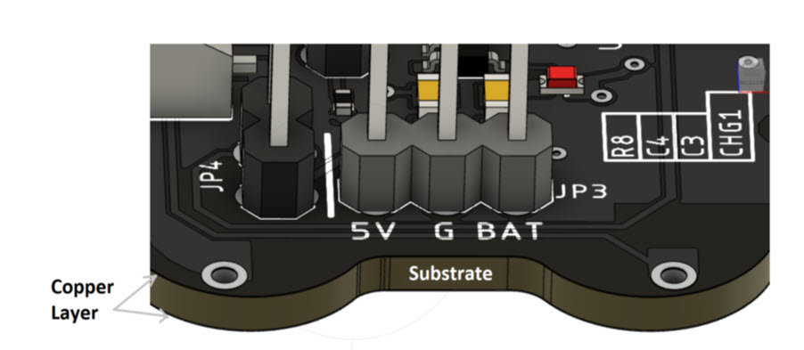
The PCB substrate is the material glued to the copper used to form the circuits on a PCB. The most common PCB substrate is a fiberglass cloth impregnated with epoxy to make it rigid.

FR4 is a common substrate which means the substrate has passed the flame-retardant test UL94V-0 (FR stands for Flame Retardant). FR4 substrates are inexpensive and can be used for circuits up to 7GHz. Higher frequency materials require other substrate materials. Common high-frequency/low-loss substrates are polyamide, PTFE (Teflon), and ceramics.
PCB substrate specifications and why they matter
The specifications for PCB Substrates can be divided into two categories: Physical and Electrical. Physical specifications include thickness, rigidity, and thermal properties such as Tg – the glass transition temperature. Let’s look at some of these physical specifications and why they matter.

Thickness and rigidity
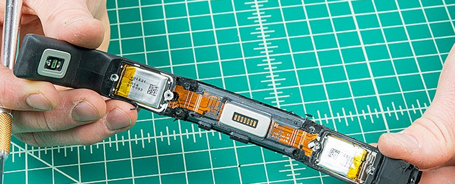
Thickness and rigidity go hand in hand. A thicker substrate bends less than a thinner one. Generally, you don’t want your PCB to bend as components could break off. 0.063” (1.57mm) is standard but thinner, and thicker substrates are available. Flex circuits are thin and designed to flex. Thickness also plays a role if you’re using microvias. The ratio of depth to diameter of a microvia is defined as 1:1 or less with a depth of 0.010” (0.25mm) or less, so, if you’re using microvias, your substrate can’t be thicker than 0.010” (0.25mm).
Tg – Glass Transition Temperature

– PCB LAB (pcb-lab.net)
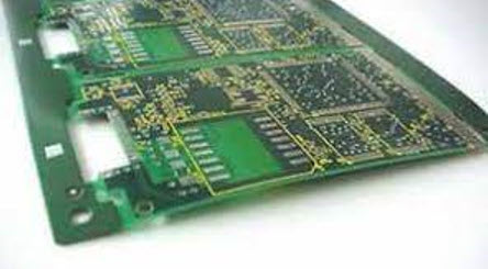
Tg is the temperature at which the epoxy impregnated in the fiberglass begins to soften. This is essential in hot environments as PCBs will deform and bend if Tg is exceeded. It can also be problematic during reflow if PCBs are exposed to temperatures above Tg for too long. PCBs with high-power devices may need a higher Tg to accommodate the heat generated by the devices.
A PCB substrate’s Coefficient of Thermal Expansion or CTE is related to Tg. CTE measures how much a substrate changes with temperature in X, Y, and Z dimensions. PCB substrates have low CTEs on the X and Y axis because the long glass fibers are tightly constrained within the epoxy. However, the CTE can be larger in the Z axis and can cause problems, like broken traces and vias, if the CTE varies significantly from the CTE of copper. Small vias are especially susceptible.
The electrical properties of substrates affect PCB’s performance as well. Let’s look at the standard electrical specifications and why they matter.
Dk, the Dielectric Constant (aka er)
The dielectric constant measures how well electric lines of force can travel through the substrate material relative to air. Permittivity is the name given to how well electric lines of force can move through a material. Some call the dielectric constant Dk epsilon subscript r (er). Dk (er) represents how much better the permittivity is compared to air, so er is called relative permittivity. Yes, it has two names, but they both represent the same thing. Think of it like sneakers and runners, two ways of describing the same thing.

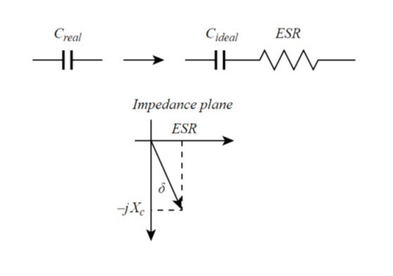
Dk will affect how concentrated and tight electric lines of force will be in a substrate. More lines of electric force mean more stored energy. And more stored energy means more capacitance. So High K substrate dielectrics result in greater capacitance. Great for power planes and ensuring good Power Integrity (PI). However, even though the substrate dielectric is an insulator, it does have resistance. And this resistance is modeled as an Effective Series Resistance or ESR. Of course, with resistance comes losses in the form of heat. This brings us to Df.

Df Dissipation Factor (aka Loss Tangent)
Df measures how much power is lost due to resistive heating. A PCB substrate forms a capacitor as an insulator with conductors usually on either side. As a capacitor, it will exhibit capacitive reactance (Xc). The phase angle between Xc and impedance reflects the amount of loss you will have. The ESR is typically relatively low, and Dissipation factors are also quite small. However, remember that Xc is frequency dependant, which results in Df increasing with increasing frequency. Substrates with a high Dk will have a high Df.
Why does Df matter?
It matters because it reflects power loss, and power loss in signals means your signals will become smaller. It also affects signal propagation times. This is especially important for highspeed differential signals and why differential traces must be equal in length.
When does it matter?
Selecting the appropriate substrate is essential when working with frequencies in the GHz range. Keep in mind that even though you may have signals in the 100s of MHz, you may have significant energy content in the GHz region if you have fast edges.
Selecting the correct PCB substrate is essential. Select too low a Tg (glass transition temperature), and your PCB may warp. Select a PCB with CTEs that differ to significantly and again warping can occur, as can break vias and traces. Signals may disappear at high frequencies if Df is too high. And while high Dk (dielectric constant) substrates provide better PI they also have higher Dfs (dissipation factors). Selecting the correct substrate will minimize these problems.
Check out the rest of the PCB Layer Stack series here:
PCB Layer Stack Fundamentals Part 1: Using Multiple Copper Layers
PCB Layer Stack Fundamentals Part 2: Routing Between Multiple PCB Layer Stacks
Looking for a comprehensive electronics and PCB design tool? Get started with a 30-day free trial of Fusion 360 today.