PCB Layout Basics Part 1: How to Place Your Components
So, you got that circuit on paper as a schematic design in Autodesk EAGLE, but now comes the real challenge. How are you going to translate all of that electrical theory into an actual physical design? These days engineers do it all, from schematic to PCB layout, and there’s no handing it off down the line for someone else to finish it up, it’s all about you. While this can present you with a new set of challenges, the PCB layout is probably one of the most exciting and rewarding parts of PCB design. It’s like a giant puzzle just waiting to be solved with some original thinking and creativity. Where do you start with all of this? You’ll need to place all of your components first.
Some Things to Know Beforehand
There are a few things you’ll want to keep in the back of your head while you go about transforming your schematic into a physical board layout, including:
PCB Layout is an Art
Many engineers see the PCB layout process as more of an artform. If you give your schematic to a hundred different engineers, then chances are you’ll get a hundred different board layouts back all with their unique characteristics. Unlike a schematic design, which is all grounded in the finality of mathematics, your PCB layout is a bit more fluid and flexible.

People can get pretty creative with just some mere traces and vias. (Image source)
Because of this, you have to remember one thing when doing your PCB layout – there’s no right or wrong way to do it. How you choose to place your components and complete your routing is all a unique representation of your design perspective. For some, this might be a bit overwhelming at first, which is why we’re going to stick with a very simple design in this blog. We’ve only got a handful of components to place, so you can take your time to place, replace, and probably do it all over again.
Just get comfortable with the whole process.
You Need to Think About Manufacturing
At the end of the day, you are likely designing a PCB to have it made physically by your manufacturer. Because of this, you need to keep several considerations in the back of your mind as you go about designing. The first is component orientation. Whenever you place like-minded components on your board, like a set of resistors or LEDs, you need to make sure they’re always facing the same direction. Why? This will make your board much easier to install, test, and inspect by your manufacturer.
The second point to consider is how you are placing your components in relation to each other. When your completed board gets handed off to your manufacturer, they’re going to send it through a soldering oven to connect all of the parts to your bare circuit board. If you have taller components that are blocking smaller ones, then chances are you’ll likely get a board back with poorly connected solder joints. When placing components, always be mindful of their size not just in your two-dimensional space, but also their height and width. For a comprehensive list of part placement tips, check out this blog.
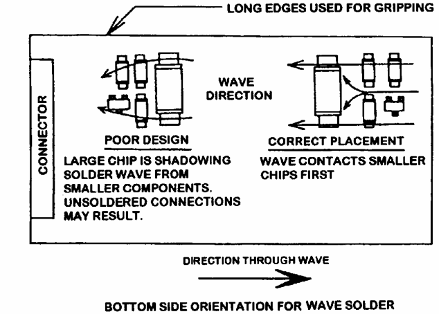
Be sure to place smaller components in front of larger ones for a reliable soldering process. (Image source)
Think About Your Routing
It goes without saying that many beginner designers make the mistake of cramming their components too close together on their first layout only to run out of space when it’s time to start routing. This happens most commonly with integrated circuits which have lots of pins that need to be connected all over your board. If you don’t give this one component enough room to breathe, then you’ll likely run out of space and will have to start your layout over again from scratch. When placing components, always be thinking about how you’ll route them, and leave enough room between parts to make that process easy.
Define Your Process
While your component placement and routing processes are filled with endless opportunities for creativity, we think it’s good to start with a structured process in mind. This isn’t meant to stifle your creativity, but to simply provide a foundation with which your creativity can grow. Once you know the limits of the walls and where you’re going, then you can be free to design as you please. The process that we’ll be using to complete the component placement process includes:
- Step 1 – You’ll first take the schematic that you finished earlier and turn it into a new PCB layout
- Step 2 – You’ll then place and rotate all of your components, working to minimize the length and crossing of airwires (more on this later).
- Step 3 – You’ll finish up your placement process by resizing the dimensions of your board layout in preparation for routing.
That’s all the details you need to know to get started. Let’s jump into some practical PCB layout strategies.
Step 1 – Turning Your Schematic Into a Board Layout
If you’ve been following along in our Schematic Basics Series, then you should have a complete schematic that looks like ours below.
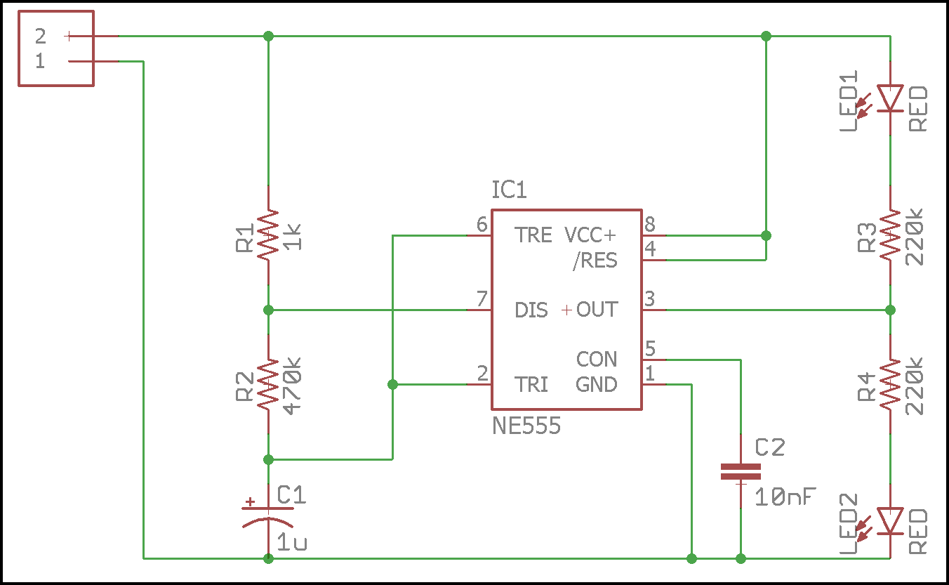
Our complete LED Flasher schematic that we’ll be turning into a PCB layout.
But if this is your first time here then be sure to read through Schematic Basics Part 1, Part 2, and Part 3 to get yourself up to speed. To convert your schematic to a PCB layout, do this:
- Open your schematic project from the Autodesk EAGLE Control Panel.
- At the top of your interface, select the SCH/BRD
 icon. This will begin the process of generating a PCB layout based on the components and wiring in your schematic.
- Select Yes if you get a warning dialog saying that the .brd file doesn’t exist and that you want to create it from your schematic.
That’s it! You should now have a second Autodesk EAGLE window open that looks similar to ours below.
When you turn your schematic into a PCB layout file, you’ll get a new window that looks like this.
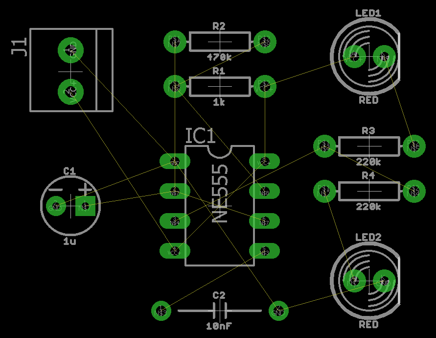
This is your blank PCB layout canvas where you will start your PCB design journey. Let’s take a moment to talk about what you see in case this is entirely new to you. Here are a few things to make a note of:
- The white square outline that you see represents the physical dimensions of your board layout. This is the area you’ll place all of your components.
- All of your components currently rest outside of this square outline. The next stage of the layout process is moving each and every piece into this area.
- You’ll also notice a bunch of lines connecting between your components. These are called airwires. You might also hear it referred to as a ratsnest. These airwires help you understand your component connectivity.
Now, let’s start moving and rotating your parts within the board space.
Step 2 – Placing and Rotating Your Components
Ok, this is where we need to start staying nimble with the directions we provide. You’ve got your blank board layout, and how you choose to place your components is ultimately up to you. In a typical PCB component placement process, most engineers will go about placing all of their edge components first, things like USB ports, power jacks, headers, etc… These parts are stuck where they are and are determined by the mechanical enclosure that the board is going to be placed inside.
After the edge components, an engineer will then typically go about placing the largest components. Things like an integrated circuit with a large number of pins will have a huge effect on what components need to be placed around it. Our example design just so happens to include an IC, and you can use this big part as the first one you place. Here’s how:
- Select the Move
 tool on the left-hand side of your interface.
- Left-click in the middle of the IC1 component and drag it inside of your board outline. You’ll notice all of the airwires move with the part.
- Now go ahead and rotate the part as you want by right-clicking. Each turn will spin it 90 degrees.
- Lastly, go ahead and left-click where you want to place your IC.
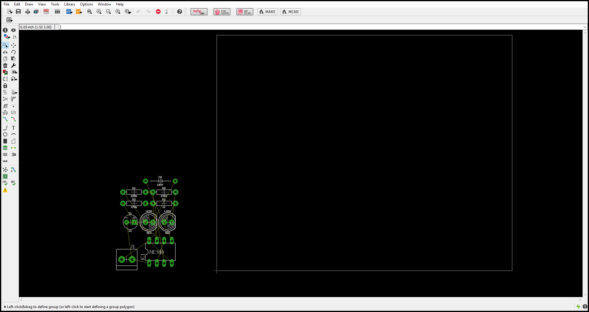
We’ve got our IC placed in the bottom left corner of our board, ready for more.
Now that you’ve got the biggest part on your layout placed, which will help a ton when placing all of your other components. The rest of the placement process is all up to you! Still not sure where to start? Here are some tips to keep in mind:
Keep Your Connections as Short as Possible
Your goal is to place all of your parts in a way that minimizes the length and cross-crossing of airwire connections between your components. Keep compatible parts together, and always remember that you can route on multiple layers, so some crisscrossing of airwires won’t kill your design.
Adjust Your Airwires Constantly
As you continue to adjust the placement of your parts, your airwires will likely need to be recalculated. Whenever you place a new part or rotate an existing one, be sure to select the Ratsnest  tool on the left-hand side of your interface to redraw all of your airwires. This tool will give you a real-time update on how your placement decisions are affecting your airwire connections.
Avoid Overlapping Parts
All of those green circles and white outlines are part of the physical package for each of your parts, and they’ll need some room for assembly. If you end up overlapping those green circles, which are going to be exposed copper on your physical board, then you’ll get an unpleasant short circuit. Be sure to always leave room between components at all times.
Have Fun!
The component placement process is a puzzle just waiting to be solved with your creative efforts. Remember, there is no right or wrong way to place your parts, just varying shades of optimization that you can discover. Take your time, and enjoy this process as much as possible. Below you’ll see how we decided to place our parts, but if it looks nothing like yours, then don’t sweat it. That’s what makes your design unique.
Does your part placement look like ours? Hopefully not, design it your way!
Note: Sometimes you might want to move a bunch of components at once. Rather than doing this individually, you can group parts and then use the move tool, here’s how:
- Select the Group
 tool on the left-hand side of your interface, then select the parts you want to group by either Shift + left-clicking each part or holding down left-click and dragging a box around your desired parts.
- All of your parts you grouped will now be highlighted. Next, select the Move tool on the left-hand side of your interface and Ctrl + right-click to move them as a group.
- Lastly, move your parts where you want them to be placed and left-click to finalize their placement.
Step 3 – Resizing Your Board Shape
Alright, by this point you’ve got all of your components placed. Did you find it creative, or maybe kind of awkward the first time around? Keep doing it again and again until you get into a component placement flow; then you’ll understand the magic. At this point, all of the hard work is done, great job! Let’s now finish up by defining the dimensions of your board layout with these steps:
- Select the Move tool on the left-hand side of your interface.
- Left-click on the top-right corner of your PCB layout outline, then drag that point towards your components to adjust the size of the corner.
- Left-click again to finalize that corner, then go ahead and repeat this process for the bottom-right and top-left corners.
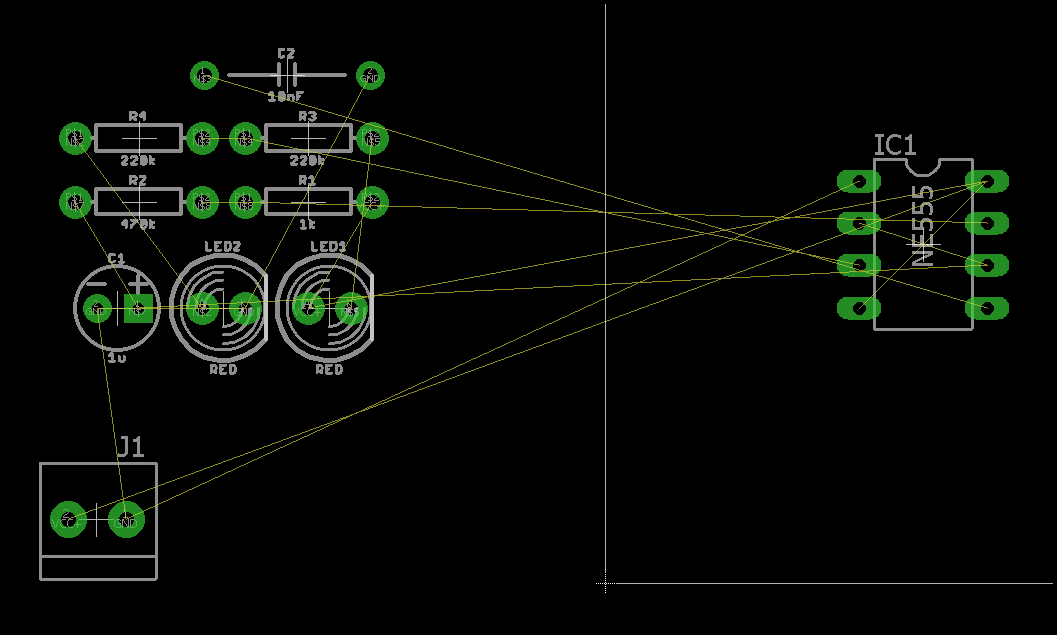
Once complete, you should have a much smaller PCB layout outline that nestles all of your components together in an efficient and compact package like the one we have below:
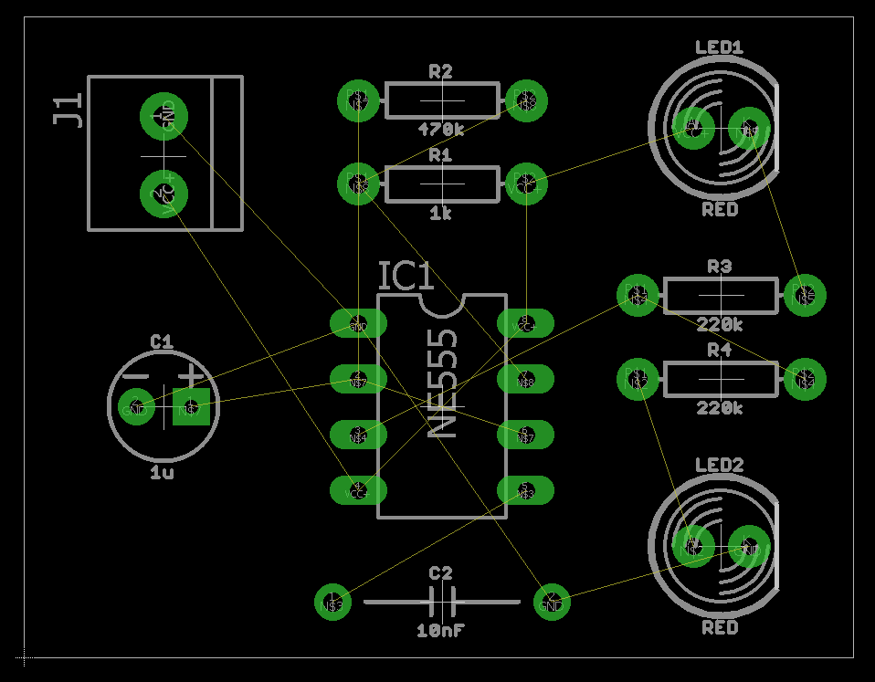
We’ve shrunk our PCB layout outline to nestle all of our parts together.
Component Placement Success
Way to go, you did it! You have now successfully placed all of the components on your very first PCB layout. There’s an old saying that goes like this – PCB layout is 90% placement and 10% routing. This is still just as true today. How you decided to place your components will ultimately determine how easy your routing job will be in the future. So did you make sure all of your airwires were as short as possible? If so, then you can expect the last 10% of your PCB layout process to be a breeze.
Chances are you might want to take a stab at your component placement process a few times just to see what kind of different results you get. The more you practice, the more you’ll start to notice the small details that can make your layout better each time. Don’t be afraid to experiment! This part of the puzzle is all about the art of engineering. Enjoy the creative endeavor, and we’re looking forward to seeing you again in our PCB Layout Basics Series. Here’s what’s up next:
- PCB Layout Basics Part 2 – Here you’ll learn how to take all of those components you just placed and route them together with traces and vias.
- PCB Layout Basics Part 3 – Here you’ll learn how to run your Design Rule Checker (DRC) and add some finishing touches to your layout with a copper pour and some silkscreen.
Making your first PCB layout in the free version of Autodesk EAGLE is just the tip of the iceberg! Get the full experience today by subscribing to Autodesk EAGLE.