It’s Like a Sandwich – How Your PCB Is Manufactured in Plain English
Curious about how that Printed Circuit Board (PCB) you just designed actually gets made? I was, until I found a bunch of videos from manufacturers on Youtube and nearly fell asleep trying to sift through all the technical details. It’s not that the PCB manufacturing process is dull in itself, there’s a ton of fascinating machinery, and a lot of human labor and love that goes into the whole mix. It’s just explained very, very dryly.
So if you’ve ever felt a bit disconnected between completing your design, sending it off to manufacturing, and wondering what happens after you get a box on your doorstep with your new PCB, this blog is for you. Let’s find out how your PCB is manufactured, in plain English with the help of a sandwich.
What Do Sandwiches Have to Do With This?
I’ll be honest, the sandwich analogy isn’t perfect. But the more I tried to think about an ideal physical representation for how a PCB is made, the more a sandwich seemed applicable. You’ve got your top and bottom layers (bread), your inner layers (meats, cheese, condiments), and everything comes together to form a completed whole.
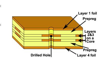
Your typical PCB layer stackup, looks just like a sandwich, kinda (Image source)
Before we get started, it’s important to know that PCBs are manufactured on giant panels, which contain a ton of other PCBs. Maybe they’re all yours, or sometimes they combine multiple designs one one panel to save everyone money. The process we’ll be talking about below goes into making a complete multiplayer board, and if you’re just dealing with 1-2 layer designs then there will be less steps involved.
Step 1 – The Shopping List
The first step in getting a PCB made starts with you. Much like assembling a shopping list for your next sandwich masterpiece, you’ll need to get all of your design files together to hand off to your manufacturer, including:
- Gerber File – This file provides all the information your manufacturer needs to know about your copper lays, solder mask, and silkscreen.
- Drill File – This file will help your manufacturer to understand the sizes and placement of every drill hole on your board
- Netlist File – This handy file will help your manufacturer to understand how all of your component will be connected together.
Once you hand off all of your design files to your manufacturer then it’s show time!
Step 2 – Selecting Your Meat & Cheese
In step 2 your manufacturer will create the inner workings of your PCB. This begins with a giant film printing machine, which creates an image of the top and bottom internal layers of your PCB.
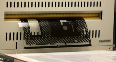
Creating the image of your top and bottom layers with a photoplotter. (Image source)
Quick side note – most fab houses don’t even use films anymore. Technology has advanced where lasers can create an image directly on a PCB, cutting out the film middleman.
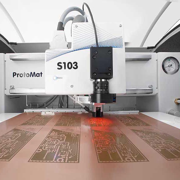
Laser Plotter at work. (Image source)
Step 3 – Combine Your Meat & Cheese Together
Next up, the created images for your internal PCB layers are laminated onto a copper panel with the help of some resin (basically industrial-strength glue). This panel is then coated with a layer of photosensitive film.
At this point a real-life human being will take the copper panel, shine a UV light on it, and let science take over to harden the photosensitive film and create your copper design patterns.
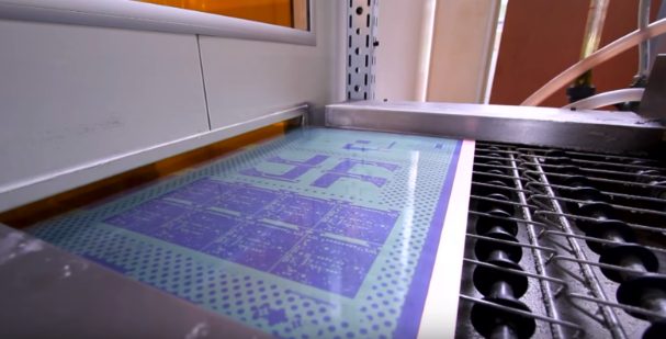
PCB images get laminated onto a copper layer to reveal your design patterns.
Step 4 – Melt That Cheese, Please
Now that your copper designs are on a panel, it’s time for a soothing alkaline bath to bring everything together! This process removes any of the extra copper hanging around, leaving only the original patterns that you created during your design process.
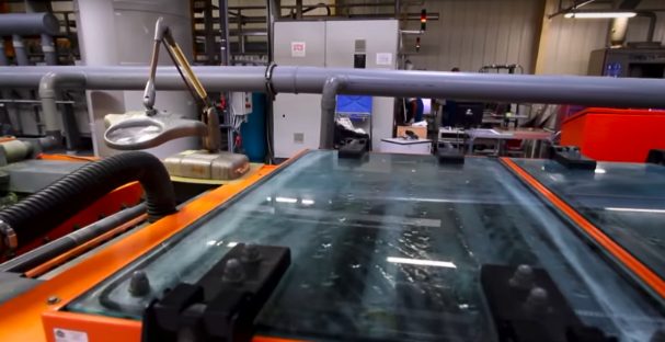
Nothing like a soothing alkaline bath to remove any extra copper on a PCB.
Step 5 – Let Everything Cool
At this point it’s time to take a glance and make sure everything is looking good. Some handy inspection software will be used to compare the newly created copper panel with your original design data to make sure everything is accurate.
Step 6 – Go Crazy with Condiments
Next, it’s time to add some of those delicious condiments to your sandwich. In this stage of the process another certified human being will take your copper panel, add some layers of foil to it, and top it off with layers of prepreg (basically a sheet of fiberglass with some glue mixed in).
This newly formed set of layers then gets bonded together thanks to some intense heat and pressure. When pulled out of the oven, these combine layers form the outer layers of your PCB!
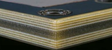
Your newly bonded PCB with layers of copper, foil and prereg.
Step 7 – Hope You Wanted Swiss Cheese
Now your copper panel gets moved over to a drill machine, which drills some holes for your through-hole components and vias. These drill machines are super fancy, and can switch out drill bits on their own.
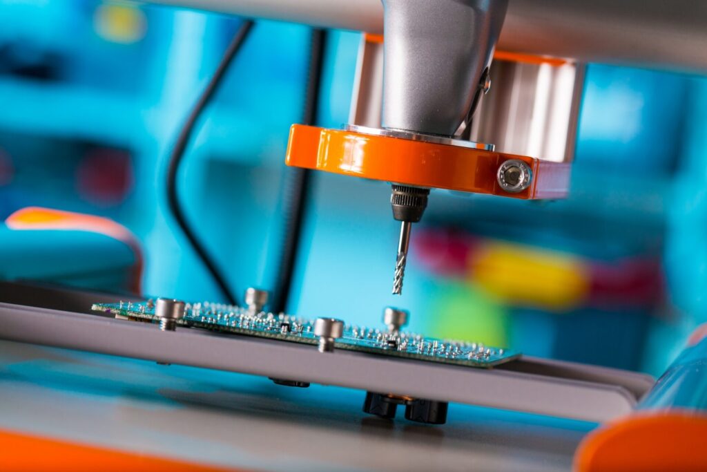
Here’s a CNC drilling machine adding some new holes to a PCB for components and vias.
Step 8 – Let It All Marinate
With your condiments in place it’s time to let everything sit and marinate together. At this stage of the process your copper panel of PCBs is given a relaxing copper bath, which coats every surface, including drill holes, with a fine layer of copper.
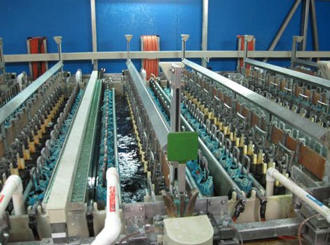
Huge copper paths coat the PCB surface with a fine layer of copper.
Step 9 – It’s Bread Time
It’s time for the bread! This process is all about creating the copper patterns on the outer layers of your PCB panel. As you slice away into a freshly baked loaf of bread to complete your sandwich masterpiece, a manufacturer will be creating images for the top and bottom outer layers of your PCB. This is the exact same process we saw in step 2.
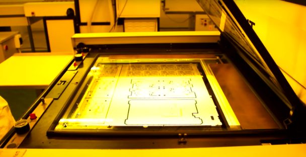
Here we are again, this time creates images for the outer layers of our PCB
Just like before, these images are laid onto your copper panel, covered with another photoresist film, and finally given some UV light to reveal your designed copper patterns.
Step 10 – Toast That Bread
Now that the outer layer copper patterns are revealed, your entire panel is cleaned in another relaxing copper bath. These PCBs have it way too easy!
Step 11 – Add Some Mayo & Mustard
We’re nearing the end of the manufacturing process here with all of our layers fully assembled. At this point a machine will apply a nice coating of solder mask to the top and bottom layers of your PCB panel. This this help to protect against rust and unintended electrical connections. Solder mask is super easy to recognize – it’s the traditional green color that many PCBs have (or blue, like an Arduino).

That trademark green color keeps a PCB protected against the elements with Soldermask.
Step 12 – Avocado Makes Everything Better
Avocado makes everything better, as does the silkscreen applied to your PCBs. Your copper panel will now be fed through a giant inkjet printer, which adds a handy legend in white print to aid with the placement of components.
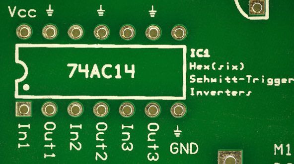
A close up of all the fine details that silkscreen adds to your nearly completed PCB.
Step 13 – Put That Sandwich Together
Alright, it’s time to put your sandwich together into a complete whole. Your bare-board PCB is ready to go, and now needs some components. Before any parts get added, your PCB panel first goes through a series of electrical tests with a flying probe or grid tester to make sure there aren’t any open or short circuits.
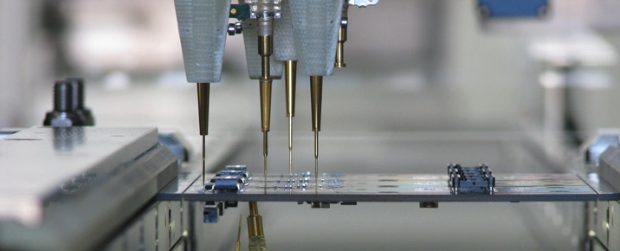
One of two ways to electrically test a PCB – the flying probe.
Step 14 – Trim Off All the Extra Stuff
We’re all engineers here, and no one likes a messy looking sandwich, so let’s trim off the excess meat and cheese and give it to the dog. As far as your design goes, the giant panel that contains all of your PCBs is now ran through a milling machine which cuts out all of the individual circuit boards.
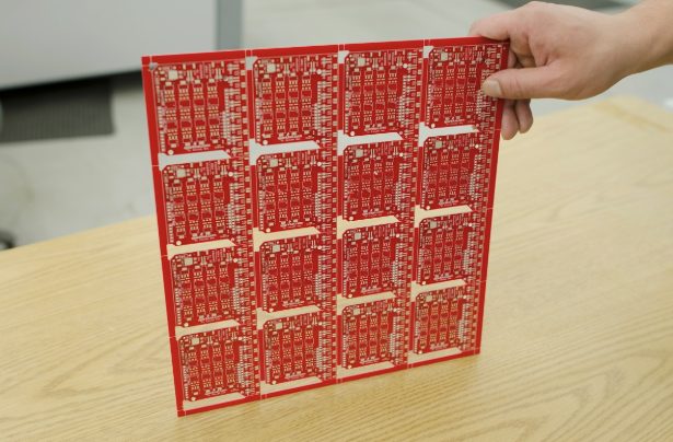
This PCB panel will run through a milling machine to piece out the individual circuit boards.
Step 15 – Inspect Your Masterpiece
Before they go adding components onto your PCB, your board will go through a final inspection process carried out by a certified human being. This person will look for any cosmetic issues including scratches and incorrect hole sizes, as well as compare your mechanical drawings to the physical board.
Step 16 – Bring On the Chips
It’s time to put some finishing touches on this sandwich masterpiece to form a complete meal! Your manufacturer will now place all of your surface mount (SMD) components on your PCB. This process uses a machine-gun like component dispenser, which can pump out over 230,000 parts per hour. Your board will then get passed through a furnace, where the solder paste will liquify and bond the the surface of the PCB.
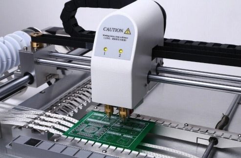
A pick-and-place machine throwing down SMD components like it’s nobody’s business.
Next, your board gets handed off to another certified human being, who will assemble all of your through-hole (THT) components by hand, including any capacitors and coils.
Step 17 – Eat It All
At long last, your sandwich and completed PCB are now ready to enjoy! At this point in the manufacturing process your board will go through its final electrical testing on a bed of contact pins. If everything checks out, it’s time to give your design a final protective layer to keep out any dust or moisture.
Step 18 – Clean Everything Up
Whew, we’re finally done. You can get to work cleaning up all those crumbs from your recently digested sandwich. On the manufacturing front, your PCB gets vacuum sealed, boxed up, and shipped to your door, or office desk.
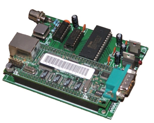
A completed PCB at last with all of its components attached!
That’s a Wrap, Folks
There you have it, the complete multiplayer PCB manufacturing process in 18 steps in plain English. Manufacturing a PCB is an incredible, process-driven endeavor that involves a ton of human labor, machinery, and science. So the next time you get your PCB manufactured, we hope you can have a better appreciation for all the love and labor that went into translating your digital bits and bytes into a completed physical circuit board.
Next time you need to manufacture a PCB, be sure to check out Autodesk EAGLE. We’ve added a new One-Click Make feature that connects with the highest quality manufacturers to get your PCB made within 24 hours, guaranteed. Try Autodesk EAGLE for free today to see how it works.