Everyday App Note: How to Reduce EMI with These PCB Design Guidelines
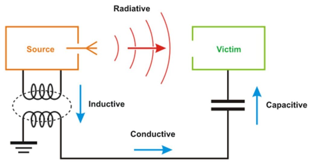
Electromagnetic Interference (EMI) is all around us, whether that’s from human-made electronic circuits or cosmic radiation in the atmosphere. In excess amounts, EMI can disrupt sensitive electronic devices. We’re not talking about your smartphone here. Think about medical equipment that’s in charge of keeping a patient alive. Or a system that keeps the trains on the right tracks in a mass-transit system.
Because of this danger we’ve developed some stringent requirements for EMI emissions in various electronic devices. FCC Part 15 is one of them. What does all of this mean for you as an electronics designer? The truth is that every electronic device emits some kind of EMI. The solution is not to eliminate it completely, but to reduce it with some well-planned PCB design guidelines. That’s what this Everyday App Note from Texas Instruments is all about.

Why Bother Reading It?
Designing a system with low electromagnetic interference isn’t impossible, but it requires a set of engineering knowledge that you might not have. Are you unknowingly creating antennas on your PCB layout that can radiate electromagnetic energy? Maybe you didn’t even know that you have to be concerned about your signal return path? You might have some problems to work on.

What’s Inside?
This app note keeps its focus practical with a ton of PCB design guidelines that you can implement right now in your design project. From ground and power planes to signal traces and shielding, say hello to your new EMI Premier. Here’s a brief sample of some of the design guidelines you’ll find inside:
Grounding Microcomputers
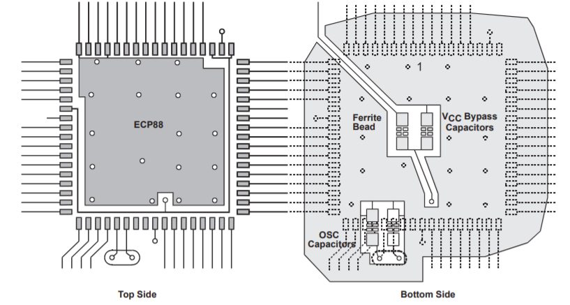
You need a ground area on the bottom layer underneath your microcomputer to act as a noise filter. This area should extend ¼ inch outside the outline of the device. The ground area also needs to provide coverage for oscillator leads and any power-supply bypassing capacitors.

Board Zoning
Thinking ahead to plan the layout of your board according to functions will help to reduce EMI. You can think of it as a floor plan, the view from 10,000 feet. High-speed logic should be kept close to the power supply, but away from slow/analog components. This ensures that the high-speed logic won’t interfere with other signal traces.

Two-Layer vs. Four-Layer Boards
When designed properly, a two-layer board can be just as effective as a four-layer board. In these layout stacks, it’s important to route returns for direct connections to the processor I/Os under the signal trace. You’ll also want to be careful to never route in isolated areas of your board, like those between high-power and digital grounds.
Read It Now
As IC devices continue to increase in speed and density, you’re bound to find all of the guidelines in this App Note useful from project to project. Get acquainted with them all today so you’ll be ready when EMI comes knocking!
Download the PCB Design Guidelines For Reduced EMI App Note now.