Everyday App Note: How to Master the Art of RF PCB Design with These Layout Guidelines
Radio Frequency (RF) devices are one of the most exciting applications to build these days in electronics design. Any up and coming technology used in smartphones, sensors, robotics, and security is going to demand these complicated, high frequency boards. But as we all know, with greater complexity comes greater headaches for engineers like you that have to design them! This Everyday App Note from Maxim Integrated will remove the black magic of RF design with some practical PCB layout guidelines.
Are You Designing an RF PCB?
RF PCBs are one of the fastest growing sectors in PCB manufacturing. With with proliferation of IoT sensors, wireless electronics, and smartphones, it’s easy to see why. But how do you know if you’re working on an RF PCB? The PCB industry considers any board that operates above 100MHz to be an RF PCB. Anything about 2GHz is a Microwave PCB.
This app note is designed specifically for the design and layout of RF printed circuit boards. These are highly complex devices that can include digital, analog, and RF components in configurations up to sixty layers! Maxim will be walking you through some of the best practices to make your design process easy to approach. Here’s a small sample of some of the guidelines you’ll find inside:
Using Vias for Transmission Line Layer Changes
Does your RF layout require you to move a transmission line between layers? Maxim recommends using at least two via holes for each transition point to minimize via inductance loading. The width of these transition vias will need to match the width of the transmission lines. Used effectively, these vias can help to cut transition inductance by 50%.
Properly Adding Line Bends and Corner Compensation
If your transmission lines need to change direction then you’ll want to use a bend radius that’s at least 3 times the center conductor width. This will ensure that impedance remains steady as current travels through the bend.
If you can’t gently curve a bend and end up with a right-angled trace, then you’ll need to use an angled miter as shown below. This helps to reduce impedance fluctuations and can be found with formula from Douville and James.
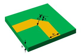
Use a right-angle bend when a curved bend isn’t possible. (Image source)
Routing on Bias and Ground Layers
The return current path for system bias layers always needs to be considered in an RF design. Adding signal layers between a bias and ground layer will create a larger return path as shown below, resulting in noise coupling on the signal layers. For the most optimal layout, make sure there aren’t any signal layers between your bias and ground return layers.
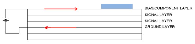
Signal layers between bias and ground will be coupled with noise. (Image source)
Download These Guidelines Now
This application note offers a ton of other practical RF PCB design guidelines that can help to make your RF project a success. These designs are just going to get more prevalent as we move into the age of connected devices, so this is the perfect toolbox to start building today! Some of the other guidelines in this app note includes:
- How to effectively layout bypass capacitors to minimize parasitic inductance.
- How to successfully implement a controlled impedance transmission line for RF power.
- How to accurately set the width of conductor traces to meet a target impedance.
Download the General Layout Guidelines for RF and Mixed-Signal PCBs App Note now!