How to Route Differential Pairs in Autodesk EAGLE
If you’re designing a high speed PCB, then chances are you’re working with the latest and most powerful technologies, like HDMI, USB3.0, Ethernet, or DDR. But with great power comes great responsibility! As a result, you’ll likely be dealing with issues like electromagnetic interference (EMI) and noise.
So what do you do about these problems? When you’ve got a bunch of noisy signals on your board and you need a way to protect the transmission of your data then you need to be using differential pairs. In this blog we’ll be looking at all of the great benefits for using differential pairs in your high speed design project, and how to route them in Autodesk EAGLE.
It’s a Dual Benefit
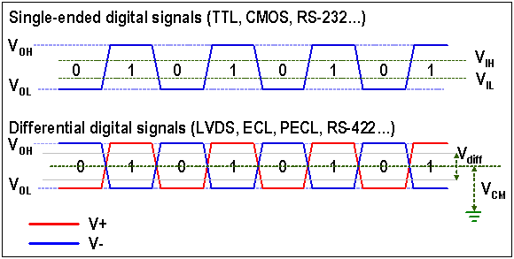
Differential pairs are the physical manifestation of putting differential signaling into action on your high speed PCB layout. Put simply, this is the process of using not just one, but two traces to transmit a signal on your board. These two traces both carry the same signal. The first trace, considered positive, carries your original signal. And the second trace, considered negative, carries the inverse of the original signal.
Why would you ever want to carry the same signal along two traces? There are a ton of reasons, such as:
- Separating power systems. Differential signals don’t typically send a return signal to ground, and because of this, you don’t need to worry about crossing over power boundaries. This can make it a lot easier to keep your power systems separate.
- Reducing electromagnetic interference. Your tightly coupled differential signals are great at resisting any EMI emissions from other noisy traces on your board layout. They also cancel out their own EMI emissions with their shared polarity and distance.
- Precisely timing. It’s also a lot easier to determine what kind of logic state a differential pair is at in any given moment. If the negative trace has a higher voltage than the positive one, then it has a higher logic state, and if it’s the other way around, then the pair has a low logic state.
While differential pairs do have a ton of advantages when it comes to resisting electromagnetic interference and noise, they also have some particular design rules that you need to pay attention to. These include:
Rule 1 – Keep differential signal traces at equal lengths. Your differential pairs are only beneficial when their lengths are kept the same, which keeps their polarity in balance.
Rule 2 – Route differential traces close together. The closer you route your differential pairs together, the less EMI they will emit on your PCB layout.
Rule 3 – Define your impedance. You need to always keep your differential pair impedance constant over its entire length. This will depend on the width of your traces, your copper thickness, and your layer stackup materials.
We’re going to avoid giving any hard and fast numbers about the design rules that we outlined above. Why? Because the constraints of your differential pairs are largely dependent on the unique composition of your design. We’ll be teaching you how to route differential pairs, but defining the details in your design rules is up to you. Ready to get started? Here’s how we’re going to break down the routing of differential pairs in Autodesk EAGLE:
- Step 1 – Define Your Net Class. You first need to create a new net class that you can use to apply width rules to your differential traces.
- Step 2 – Define Your Net Names. You then need to change the name of your nets, so Autodesk EAGLE recognizes them as differentials.
- Step 3 – Apply Your Net Class. You’ll then apply the net class you created in Step 1 to each of your nets.
- Step 4 – Route Your Differential Pairs. Lastly, you’ll use the Routing tool in Autodesk EAGLE to route your differential pairs to their intended destination.
Step 1 – Define Your Net Class
Before you start routing any differential pairs, it’s a good practice to create a net class that can control the width of your traces. Net classes come in really handy when you want to apply the same set of rules for widths, drill sizes, and clearances for a group of nets on your board. Here’s how to do this:
- Open your PCB layout (.brd) file from the Autodesk EAGLE Control Panel.
- Select Edit at the top of your interface, then choose Net classes to open the Net classes dialog.
- Next, give your net class a name, then specify a width value. In our example, we’re giving our net class a name of “diff pairs” and a width of 16 mils.
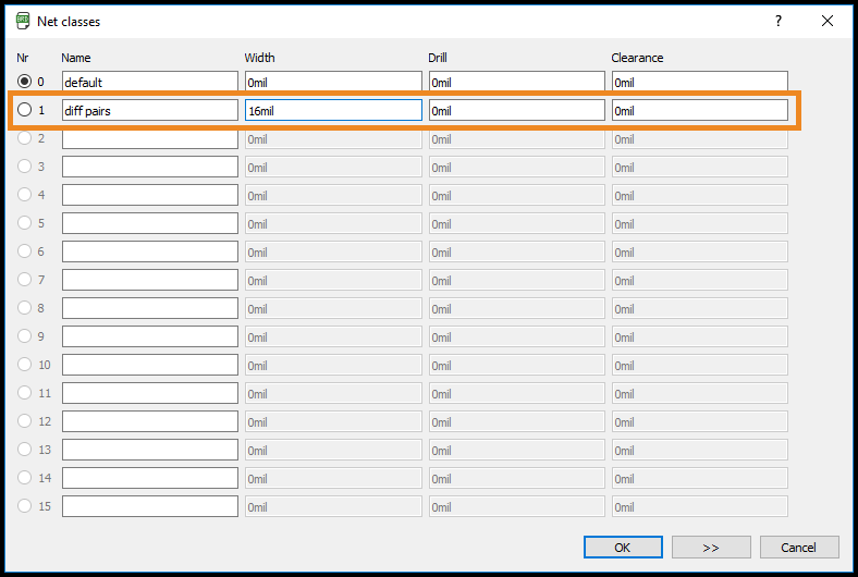
- Once your values are added select OK to save your newly created net class.
Step 2 – Define Your Net Names
This is the most important step of setting up your nets to be routed as differential pairs. Autodesk EAGLE recognizes differential pairs by looking for matching net names. These net names need to meet three requirements:
- The net names need to be identical; except a suffix on each net.
- The positive net needs to have a “_P” added to the end of its name.
- The negative net needs to have a “_N” added to the end of its name.
Without these requirements in place, Autodesk EAGLE won’t recognize that you want to route a differential pair and will respond as it normally would when routing – by connecting only one of the nets. Here’s how to change your net names:
- Select the Name
 tool on the left-hand side of your interface.
 - Left-click on your first net to open the Name dialog.
- Enter a name in the New name: field and be sure to end it with _P. Then select OK to confirm the name.

- Repeat this same process for the second net, giving it an identical name and adding _N at the end.
In our example, we named our nets DIFF_P and DIFF_N. Notice how the names are exactly identical, with the only difference being the _P for positive and the _N for negative. That’s it, now that you have two identical net names with their unique designators, and Autodesk EAGLE will automatically recognize that you’re trying to route a differential pair.
Step 3 – Apply Your Net Class
The last and final preparation step before routing is to apply the net class that you created in Step 1 to your two nets. Based on the class we created, this will constrain the width of our two differential traces at 16 mils.To apply your net class, do this:
- Select the Info
 tool on the left-hand side of your interface, then left-click on your first net to open the Properties dialog.
 - Next, left-click the Net Class dropdown and select the new net class that you created in Step 1.
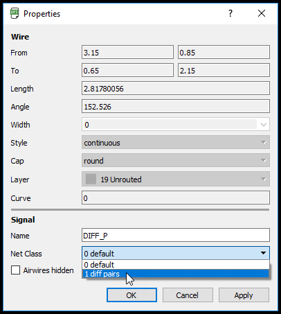
- Last, select Apply to save your changes and then select OK to close the dialog.
Step 4 – Route Your Differential Pair
Alright, all of the prep work is now done for the two nets you want to route as a differential pair, let’s do it! This process will use the same Route tool that you’ve always used to route nets on your PCB layout.
- Select the Route
 tool on the left-hand side of your interface, then left-click on your first net.
 - After left-clicking, you should have two differential pair traces extending out from your two nets. Now drag your traces as you normally would towards their end destination.
- When you reach the net you want to connect to, left-click to finalize the connection of your differential pairs.
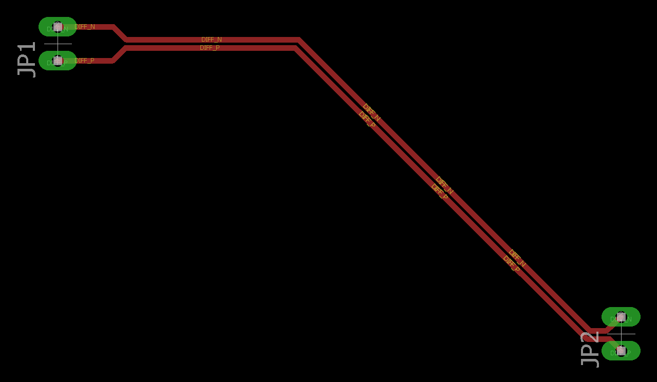
That’s all there is to it. You have now just routed your very first differential pair in Autodesk EAGLE, take that EMI! Did everything go according to plan when you followed the steps above?
Note: If for some reason you tried to route and only got one trace instead of two, then double check to make sure that your net names are identical and have their respective _P and _N extensions.
No EMI, No Cry
Differential pairs are a great tool to add to your electronics toolbox whenever you’re working on a high speed design. They help resist incoming and reduce outgoing EMI, and ensures that signals get to the receiver with any cross-talk. And not only that, using differential pairs makes it easy to determine the signal’s logic state, and they even have a lower voltage requirement than using single-end traces! Be sure to take advantage of them the next time you find yourself working with those modern and powerful technologies like HDMI, USB3.0, Ethernet, and more!
Ready to start using differential pairs in your own high speed design project? Try Autodesk EAGLE for free today!