PCB Layout Basics Part 2: How to Route, or Autoroute, Your PCB Design
If component placement is a work of engineering art, then routing can be understood as a puzzle just waiting to be solved! Are you the puzzle master that is going to rise to the challenge in PCB Layout Basics Part 2?
In Part 1 of our PCB layout series, we walked through the process of placing components on a simple LED flasher project. Now that you’ve placed all your parts on your PCB design, it’s time to start connecting your components together with traces. Just like component placement, routing is an equally creative endeavor that will tap into both your scientific and artistic skills. You’ll be working with precise trace angles, specific clearances, and mathematical copper calculations. And once you’ve got the details defined, you can then turn on the artistic side of your engineering mind and get down to connecting your beautiful puzzle together.
Ready to get started? Let’s look at how you can either manually route, or autoroute, your PCB design.
Before We Start
Before we get started with PCB routing, there are a few things you need to know about how Autodesk EAGLE can make your life easier, and also how the autorouter works. Remember these details before you start your journey:
Let Your Tool Help You
The worst thing you can do during your routing process is connect nets incorrectly, but Autodesk EAGLE makes this process easy with some handy highlighting. Check out all of the airwires in the image below; they define connection paths between components.
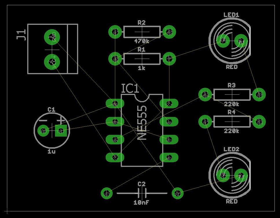
All of these airwires show exactly what nets need to be connected. Another way Autodesk EAGLE makes your job easier!
If we go ahead and select the Route ![]() tool in Autodesk EAGLE and then select a green net, you can see what happens in the image. All elements that belong to the net are highlighted in bright green, giving you an easy to follow map of your locations for your routes.
tool in Autodesk EAGLE and then select a green net, you can see what happens in the image. All elements that belong to the net are highlighted in bright green, giving you an easy to follow map of your locations for your routes.
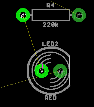
The bright green nets show which two pads need to be connected when routing.
Use the Autorouter Wisely
The autorouter is a very useful tool when used wisely. However, it’s by no means a replacement for getting your hands dirty and routing your board. What are some of the great applications for the autorouter in Autodesk EAGLE?
- Optimizing Placement. After placing all of your components, you can then use the autorouter to see how optimized your components are placed. If the autorouter returns a completion result of 85% or greater than you know you did a good job of placing your parts. If not, consider pushing your parts around.
- Discovering Bottlenecks. You can also use the autorouter to identify bottlenecks and other critical connection points that you might have missed when placing your components. Maybe you packed a couple of ICs too close together. Your autorouter can show you where you might need to leave more space between components.
- Getting Inspired. Getting stuck on a section of your design that you don’t know how to route? You can always fire up the autorouter to see how it takes care of the job, then try routing that same spot yourself with your new perspective. You might just find a strategy for your traces that you didn’t see before your autorouter gave it a try.
Outside of those three uses, do not to rely on your autorouter as a complete replacement for manually routing your board layout. This holds true especially as your designs start to get more complex. Instead of forming an unhealthy dependency on your autorouter from the get go, just know that it’s meant to be used in specific situations to augment your abilities, not replace them.
Let’s dive into the finer details of routing including:
- How to manually route on a single layer.
- How to manually route on multiple layers.
- And how to delete trace segments while or after routing.
Routing Your Board With the Autorouter
Let’s experiment with the autorouter now:
- Open your PCB layout (.brd) file from your Autodesk EAGLE Control Panel.
- Select the Autorouter
 tool on the left-hand side of your interface to open the Autorouter Main Setup dialog.
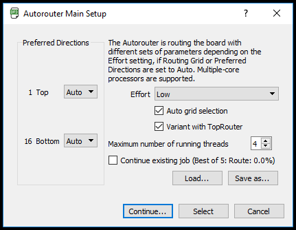
You’re in complete control of the autorouter setup with settings for effort, CPU threads, and routing directions.
- There’s quite a few settings here that you can adjust, like routing directions, effort, and the number of threads to use in your CPU. Feel free to change these settings, but we will leave the settings to their default, then select the Continue… button.
- Within the Routing Variants dialog, you’ll see a list of all the routing variations the autorouter will attempt. Select the Start button to begin the autorouting process.
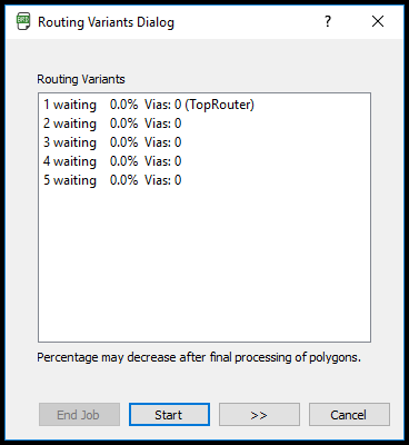
Autorouting on a low effort mode produced five potential routing variations that the autorouter will attempt.
- Once the routing is complete, select the Evaluate button, and you’ll see your completion percentage in the bottom-left corner of your interface.
How did your router do? This is a pretty simple design so your autorouter should get to 100%. On more complex designs, you can expect this number to be lower. As you can see, the autorouter can do a decent job on a simple design like your LED Flasher, but you won’t be making simple designs forever, so let’s learn how to route manually. Press Ctrl + Z (Cmd + Z on Mac) to Undo your autorouter’s work.
Tip: To unroute your board without using the Undo, you can use the RIPUP command. Just type RIPUP ; in the command line and all of your routed traces will convert back to airwires.

The RIPUP ; command is so helpful!
Manually Routing Your Nets
The process for manually routing in Autodesk EAGLE is straightforward. Your job is simply to connect the airwires together that Autodesk EAGLE highlights for you. But the challenge is figuring out how to connect all of them without any overlapping connection points (shorts). Here’s how to connect a trace between two nets:
- Select the Route
 tool on the left-hand side of your interface.
 - Next, press Spacebar to cycle through the available routable layers. You can also select your desired routing layer in the top-left corner of your interface with the Layer Selection dropdown.
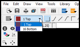
Press Spacebar before creating a trace or use the layer dropdown to select the layer you want to route on.
- Once your layer is selected, left-click on your first net to start your connection. You’ll notice that Autodesk EAGLE will highlight that net and the pads to connect.
- You can now drag your mouse towards the next net, and your trace will follow your cursor. By default you’ll be using a 90-degree trace, if you right-click, you can change your trace angle to a different angle.
- Once your trace reaches its net destination, left-click to finalize the connection.
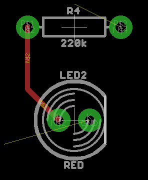
We have our first net connected between R4 and LED2. Notice the airwire is now gone.
After finalizing your net connection, the airwire that you were following should have disappeared. You can go ahead and repeat the five steps above now and see how far you can get with routing your board.
Multilayer: Manually Routing Your Nets with Vias
While you can probably use your basic routing skills to get most of the work done on this simple design, you might run into a few rough spots where you need to use a via. Why would you need to use vias though? They’re ideal for situations where you don’t have a way to connect a trace without having it intersect with another trace, which can end up creating a short on your board. By using a via, you can instead go under or above this existing trace by connecting a signal between the top and bottom layers of your board. Here’s how:
- First, select the Route
 tool on the left-hand side of your interface and begin your routing process.
 - After left-clicking your first net and dragging out your trace, press Spacebar to automatically add a via to the end of your trace segment.
- Take a moment here to look at the via options at the top of your interface. You can change the shape or your via along with its diameter and drill size. Adjust these as you need.
- Now go ahead and left-click to place your via, and continue to drag out your trace. You’ll notice that it’s now a different color, signifying that you’re routing on a different layer of your board.
- Go ahead and drag this trace to its final net connection, and left-click to finalize the placement.
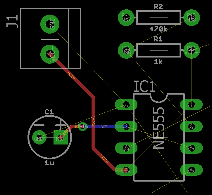
Here’s an example of a via in action. We could have also started routing directly on the bottom layer from C1.
There you go, you now know how to place down a via when you’ve got yourself into a tricky routing situation.
But what happens if you make a mistake while routing?
Deleting Your Traces
You now have two of the primary tools you’ll need to successfully route your PCBs of varying complexity – the essential Route tool and the Route tool with the addition of vias. Now it’s time to learn how to delete traces. You can remove trace segments one of two ways – either by deleting while routing, or deleting after routing.
Deleting While Routing
Removing trace segments while you route comes in very handy when you need to make adjustments on the fly without getting out of routing mode. Let’s try it:
- Begin your routing process by selecting the Route
 tool then left-clicking a net and dragging out a trace.
 - Next, left-click anywhere on your board layout a couple of times as you drag out your net to add some new segments.
- To undo these segments, simply press Backspace. You’ll notice that the last segment you placed gets removed. And you can keep pressing Backspace to remove the other segments you placed.
Deleting After Routing
If you’ve already finished your board layout and need to make some needed adjustments, then you’ll want to use the Ripup tool to remove unneeded trace segments with these steps:
- Select the Ripup
 tool on the left-hand side of your interface.
 - Left-click on a trace to remove the selected segment. You can continue left-clicking to on each segment to continue to remove them as needed.
- If you delete a segment on accident, just press Ctrl + Z (Cmd + Z on Mac) to restore it.
You’ve Got All the Tools You Need
You now have all the tools you need to successfully complete your board layout! You learned how to do some basic manual routing with traces and vias, and also how to delete traces both during and after your routing process. Now’s your chance to get creative. Spend as much time as you need connecting all of your airwires together on your PCB layout to solve your routing puzzle.
Becoming a Puzzlemaster
So did you master your PCB layout puzzle? Remember, there’s no right or wrong way to complete this stage of your PCB layout process, which is also what makes it so challenging. It’s a unique representation of your engineering creativity. What matters most is that all of your nets are properly connected.
If it doesn’t, then try again and again! Just like the component placement process, every time you route your board you’ll get a different result and a deeper level of confidence. And the more you practice, the more you’ll start to see the intricate details and pathways that your traces can take that you never realized before. At this stage, your PCB design software process is largely complete. The only remaining parts to do is check your design for errors with a Design Rule Check (DRC), and add some finishing cosmetic touches. Join us for PCB Layout Basics Part 3 to learn all about this and more!
Making your first PCB layout in the free version of Autodesk EAGLE is just the tip of the iceberg! Get the full experience today by subscribing to Autodesk EAGLE.