& Construction

Integrated BIM tools, including Revit, AutoCAD, and Civil 3D
& Manufacturing

Professional CAD/CAM tools built on Inventor and AutoCAD
8 min read
Imagine this, you just ordered yourself a brand new computer, and you can’t wait to get it all set it up. But instead of receiving a small box on your doorstep from Amazon, you have a delivery truck backing in with pallets to deliver. And not only that, but there’s also a bunch of support technicians walking into your house. From what they said, it sounds like they’ll be there for a few weeks to get this new computer of yours up and running.
While this might seem crazy by today’s standards, it’s exactly what the process for setting up a computer was like in the 1940s. And good luck fitting those things in your home, computers in the 1940s often took up an entire room, weighed many tons, and required constant air cooling to keep all of their vacuum tubes working.
Point being, the small computers that we know today, the ones that we can slip into our backpacks, or fit in our pockets, or strap onto our wrists, are just a shadow of the beasts from yesterday. And this entire miniaturization process that we’re all reaping the rewards from would have never been possible without semiconductors.
You might have encountered vacuum tubes in older electronic equipment if it survived from the mid-1900s. They were all over the place, being used in radios, televisions, radar equipment, and telephone systems. Vacuum tubes are what you might expect, a glass tube enclosing a set of components where all of the oxygen has been vacuumed out of the space. What’s so special about these tubes? As Thomas Edison found out in 1883, you can get a current to travel through a vacuum tube. And when you force it to move only in one direction, then you’ve created yourself a diode.
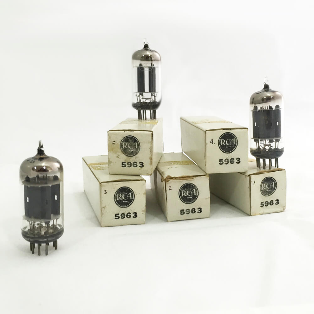
The old 5963 vacuum tubes, still in use today! (Image source)
The ability to control the direction of current was imperative for devices like radio sets, which needed to transform unpredictable alternating current (AC) into something more smooth and stable in the form of direct current (DC). Vacuum tubes did just that. And as vacuum tubes become more advanced you could start to control the flow of not one, but two current sources within a single tube, thus you create a switch.
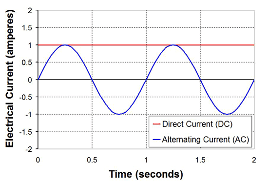
The difference between AC and DC, as you can see DC is much more predictable. (Image source)
See where this might be going? With vacuum tubes using a heated cathode, plate, and control grid as shown in the picture below, you could use the center grid to control the flow of electrons to be either positive or negative. And if there’s anything to know about the basics of digital electronics, it’s that everything is based off 1s and 0s, or on and off, or positive and negative.
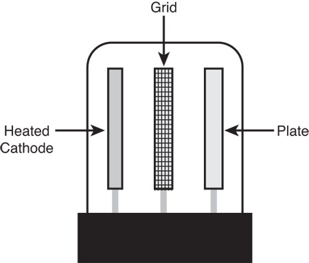
The internal parts for a triode vacuum tube that provides for the back and forth control of electricity. (Image source)
So with this simple vacuum tube, the possibilities for modern computing were born. But that doesn’t mean vacuum tubes were perfect, quite the opposite in fact. Here are just a few of the problems they faced:
As you can see, it wasn’t easy working with vacuum tubes, or being the one that had to fix them when they broke. And while they did introduce us to the modern concept of digital computing, they were also power hogs, and pumped out enough heat to require a cooling system to be ran 24/7. In later computer systems, you could expect a vacuum tube to fail every couple hours. It’s pretty clear that we needed a better solution.
It was the invention of the transistor in 1947 by Bell Laboratory inventors John Bardeen and Walter Brattain that finally saved us all from vacuum tube craziness. This little device didn’t have any of the moving pieces that could shatter glass and was instead considered a solid-state device that was way smaller consumed less power, and was much quicker than vacuum tubes.
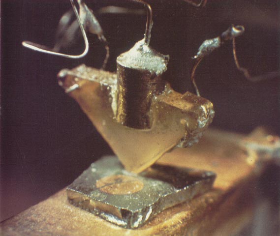
The first transistor invented by Bell Laboratory inventors John Bardeen and Walter Brattain. (Image source)
Essentially, we went about finding a way to miniaturize the vacuum tube, and in the process took out all of the tube’s blemishes while retaining its purpose – to allow us to control the flow of electric current which forms the basis of digital electronics. These days you’ll find transistors in every electronic device. If it has an Intel Core i7 process inside, then that thing packs in 731 million transistors inside a tiny space.
Now you might be wondering, how in the world did we go from glass bulbs in a computer that filled an entire room to millions of transistors in devices that can fit in the palm of your hands? It all started with semiconductors and a massive amount of research.
You’ll find semiconductors powering every kind of microprocessor chip around the world, including transistors and diodes. All of these components and chips are made from silicon. Here’s the problem with silicon though – if you pull it up on the periodic table, you’ll notice that all of the outer electrons are in perfect balance and won’t move around. This means silicon is a natural insulator.
So in a process called doping, you can turn silicon into a decent conductor. And when you have doped silicon, you’ve created what we all know as a semiconductor which can be manufactured to create transistors, integrated circuits, and microprocessors. Inside all of these silicon-based parts is the same foundation, a solid-state switch that you can use to create boolean logic gates, all of a fraction of the size of a vacuum tube. This doping process includes two flavors:
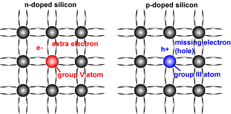
N-Type and P-Type doping in action, one adds an extra electron, the other removes one. (Image source)
Of course, this doping discovery didn’t happen overnight, and there wasn’t some scientist that randomly spilled some impurities in silicon and suddenly figured it all out. It took a lot of research to understand how all of this doping worked, and we have Esther Conwell to thank for this incredible breakthrough.
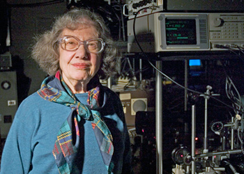
The legendary semiconductor researcher Esther Conwell. (Image source)
This brilliant woman was an American chemist and physicist who spent a great deal of her time studying how electrons move around within silicon that has been doped with impurities. The bulk of her research was done during her master thesis under the guidance of Victor Weisskopf, an American theoretical physicist. Both Conwell and Weisskopf uncovered exactly how materials affect the movement of electrons inside transistors and integrated circuits, all of which were made of doped silicon.
When Conwell finished her master’s thesis, she then went on to work at Bell Labs where she studied the effect of high electric fields on electron transport in semiconductors. Conwell was investigating how high energy fields could cause electrons to change their movements in unintended ways, which would drastically affect the performance of electronic devices.
Without Conwell’s countless years of research, we would never have advanced our understanding of semiconductors, and things like smartphones, medical equipment, or satellites might have never been possible. Conwell went on to earn a ton of achievements and recognition for her groundbreaking research, including:
We just don’t have Esther Conwell to thank for her research; we have her to thank for creating an entire foundation of knowledge for the future of the semiconductor industry. With all of her dedicated work, we might still be living in a world of vacuum tube computers, and that’s a world no one wants to live in.
These days semiconductors are everywhere, all thanks to the research done by Esther Conwell. I can’t even imagine what life would be like today without semiconductors, can you? We certainly wouldn’t have devices that can fit in the palm of our hands, and good luck toting around a computer that takes up the size of a room. It’s not just consumer computers that semiconductors have impacted; there’s also medical diagnostic equipment, rockets, electric vehicles, and so many more beautiful advancements that have made this world a better place.
During the past 50 years, we’ve taken the research done by Conwell and the advancements made by manufacturers to create the remarkable world of electronics. And with devices that are smaller, faster, and more reliable than ever, there’s no saying what we’ll see next. Maybe quantum computing will be the next evolution in our electronics world? If it is, who will be the pioneer researcher that is going to push that path forward, just like Esther Conwell did for semiconductors? Only time will tell.
Ready to make history yourself? Turn that idea of yours into reality! Try Autodesk EAGLE for free today.
By clicking subscribe, I agree to receive the Fusion newsletter and acknowledge the Autodesk Privacy Statement.
Success!
May we collect and use your data?
Learn more about the Third Party Services we use and our Privacy Statement.May we collect and use your data to tailor your experience?
Explore the benefits of a customized experience by managing your privacy settings for this site or visit our Privacy Statement to learn more about your options.