Ever wonder what kind of Design for Manufacturing (DFM) mistakes you can make that will drive your PCB manufacturer absolutely crazy? Learn about the top 10 DFM mistakes now, so you don’t make them in the future!

Listen we get it, designing a PCB layout is hard. Especially when you’re trying to smash in all of that functionality into an enclosure that seems to shrink more and more with every new board design. You’ll likely end up having a manufacturer breathing down your neck at the end of the line, telling you that this is too small, that’s too thin, and that component doesn’t match. Aren’t you just tired of the back and forth? Guess what, so is your PCB manufacturer!
Design for Manufacturing
This is where Design for Manufacturing (DFM), can make everyone’s life easier. Think of it as a kind of risk management. It’s personal insurance that what you spend hours designing can actually be made at the end of the day.
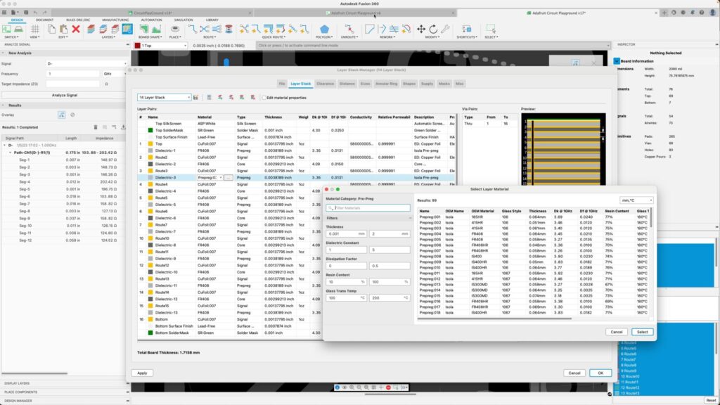
Whether you like it or not, you can make the best PCB in Autodesk Fusion 360, but if that board can’t be made, then it’s all for nothing. So instead of fighting with your PCB manufacturer for each and every mm, just start your design process off right by not making these 10 DFM mistakes.
1. Not leaving enough edge clearance
The problem with copper is that while it might be a great conductor, it’s also prone to corrosion from the environment. To combat this, your manufacturer coats it with a protective material. But what happens if you don’t leave enough space between the edge of your board and your copper? That protective coating can get cut off in the manufacturing process. This exposes the copper beneath, and then you’re just waiting for a disaster to happen.
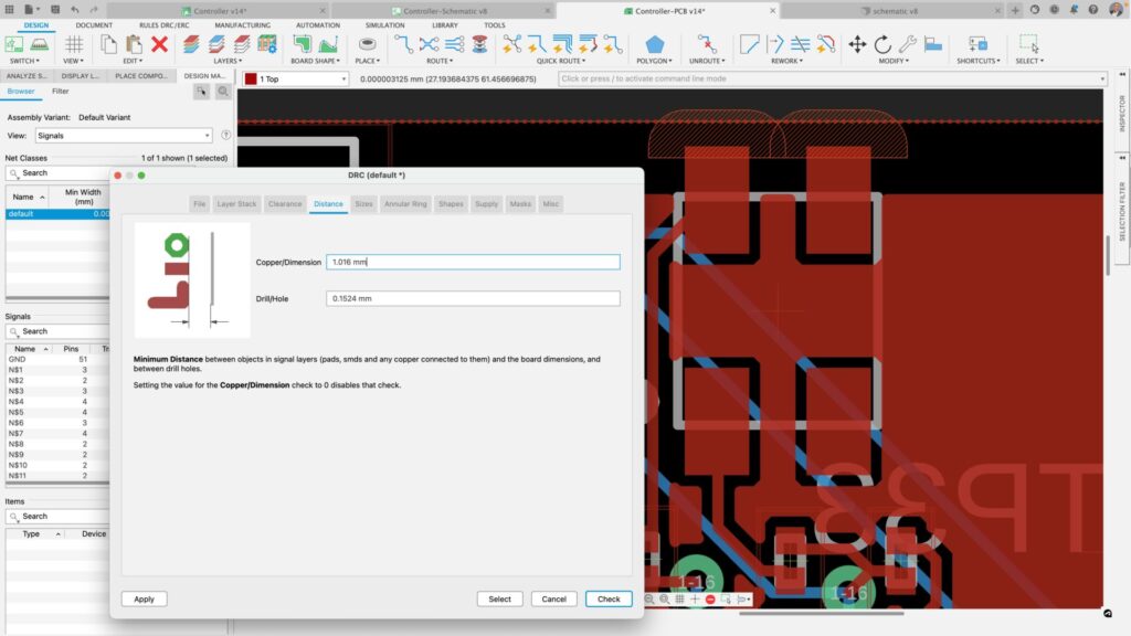
This problem is an easy one to fix. Ensure that you’re leaving enough space between the edge of your copper and the edge of your PCB. That’s a minimum of 0.010” inches for outer layers and 0.015” for inner layers. You can even plug these clearances into your design rules (DRC), so you’ll never need to worry about it again.
2. Making acid traps
We all likely know by now not to use any acute-angled traces in our PCB layout, opting instead for 45-degree angled traces instead of 90. This helps to prevent any acid from getting trapped during the PCB etching process. It also helps to prevent any serious circuit defects down the road.

But time and time again, PCB designers forget one simple thing — you can still make acute angle acid traps from the joining of two traces. Do yourself a favor and thoroughly scan all of the trace angles on your board after you finish your routing. Are you unintentionally creating an acid trap from the joining of two traces even if you used 45-degree routes? It happens, but fix it before your manufacturer ever gets your design files.
3. Placing vias in pads
It can be really tempting to throw a via inside a pad when your board space is getting tight. However, when it comes time for soldering, that via-in-pad will actually draw solder away from the pad, causing the attached component to be mounted poorly.
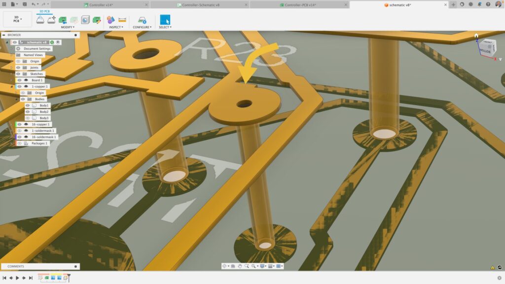
While this one-off special technology is certainly useful in the right circumstances, only use it if it’s absolutely necessary. This also holds true for micro vias, blind vias, and buried vias. If there’s an alternative, use it!
4. Overcomplicating Your Board Layout
If you’re struggling to place all of your SMT components on the same side of your board and are thinking of placing a few on the bottom, stop. This going to cost you twice as much, and is going to be a pain for your manufacturer to run your board not once, but twice, through their pick and place machine.
No one likes throwing money away during manufacturing. Take the time during your PCB layout process to place all of your SMT and through-hole components on the same side of your board. Your manufacturer will thank you later, and so will your wallet.
5. Sending an incomplete pick and place file
Chances are if you’re placing SMT components then you’ll need to send your manufacturer a pick-and-place file. This file tells a pick-and-place machine exactly where every part needs to be placed on your board. But when was the last time you verified the data this file generates? And is it even complete?
It’s a manufacturer’s worst nightmare when the pick and place file a designer sends over doesn’t include all the information they need to place parts properly. At the very least, be sure to include the following:
- Component Reference Designator (e.g., C1)
- Component Part Number (e.g., 100CAP0001)
- Component Description (e.g., C04020 1uF Electrolytic)
- Manufacturer Part Number (e.g., CRD0402D10L)
- Mid Point X(mm) (e.g., 10.242)
- Mid Point Y(mm) (e.g., 23.750)
- Orientation Angle (e.g., 290)
- PCB Layer Side (e.g., Top)
6. Not Verifying Your Layers
You might think that your design process is done once you mash the generate button on your Gerbers, but hold up! There’s still another step to take. Manufacturers occasionally get shipped Gerber files with board layers that don’t even match up, because we all know a 30-year-old file format isn’t perfect.

Before sending your design files off to your manufacturer take the time to open them in a free third-party Gerber viewer to ensure that all of your layers match up. If they don’t, then you’ll likely need to generate your output documentation again or make some adjustments to your layout.
7. Using Multiple Tool Sizes
We all need drill holes and vias on our boards, but are you the one that decides to make half of your holes 37 mil, and the other half 38 mil? Why? This requires another set of tool sizes that your manufacturer has to swap in, eating away at your wallet.
Instead of having multiple holes and via sizes, just keep them all the same. For standard 0.062” material you can use a via hole size of 13.5 mil and a drill hole size of 37 mil. Having the same size for holes and vias will make it easy if you need to add more in the future.
8. Putting Silkscreen on Pads
We know, you’ve got a ton of different layers on your board, and it’s easy to miss if you accidentally place your silkscreen on top of a pad. But what you might not know is that having silkscreen on a pad can make the soldering process a lot more difficult for your manufacturer.
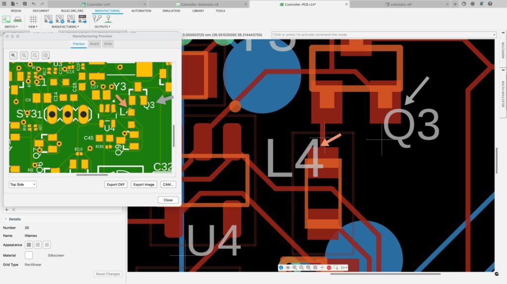
Always avoid silkscreen on pads for a smooth soldering process.
As a general rule, always keep your silkscreen at least .003” away from your solder mask. And when you’re double-checking your PCB layout at the end of your design process, make sure that you have all the layers turned on in Autodesk Fusion 360. This will show you the full dimensions of your pads.
9. Not adding solder mask between pads
Solder mask has the important job of insulating all of your copper from accidental contact with other metals. If you don’t place any solder between your pads, you’re waiting for an opportunity for a solder bridge to form. And then you’ll be wondering why your PCB keeps short-circuiting.
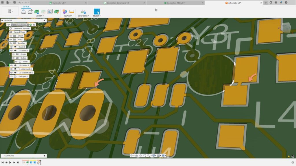
To prevent this from happening, always make sure that you define your solder mask requirements in your design rules (DRC). This is especially important when you’re carrying settings over from a larger board to a smaller one. And if you’re working with tightly spaced components like small pin pitch devices, give your PCB layout a double check for solder mask placement before sending any files off to your manufacturer.
10. Adding the Wrong Size or Shaped Footprints
Are you sure that the component you added to your Bill of Materials (BoM) will fit on the pad you placed on your PCB? If you’ve got the wrong-sized footprint for your component, then you’ll likely wind up with parts that break during assembly or don’t properly solder.
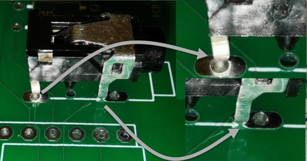
When making footprints for your parts, always ensure that you’re designing them to IPC standards. This way your physical parts and footprints will always match, and you won’t run into any unnecessary delays during assembly.
Design for Manufacturing – Risk Management Starts at Design Time
Design for Manufacturing (DFM) was never meant to be a post-design checklist that you consult once your PCB layout is finished. Rather, DFM is a method of designing at design time, by always keeping your manufacturer’s constraints in mind. Working this way won’t just make your manufacturer’s life easier, it will make yours easier as well. After all, do you really enjoy the back-and-forth emails and phone calls because you forgot your solder mask between pads, or you decided to use 5 different sizes for your visa? When in doubt, always take a Design for Manufacturing approach to your next PCB design. It’s like risk management, and it always starts at design time.
Get Started with Design for Manufacturing
Ready to design a PCB with your new Design for Manufacturing (DFM) knowledge? Start with a free 30-day trial of Autodesk Fusion 360.